
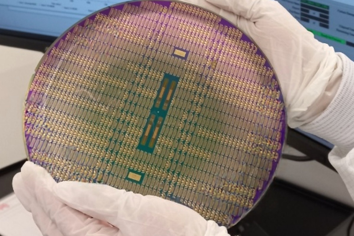
PMUT Custom Platforms
High-performance piezoelectric micromachined ultrasonic transducers and dense arrays.
View Platform →From engineering samples to wafer-scale production.
Choose a platform to explore dedicated capabilities, delivery formats and design support.
High-performance piezoelectric micromachined ultrasonic transducers and dense arrays.
View Platform →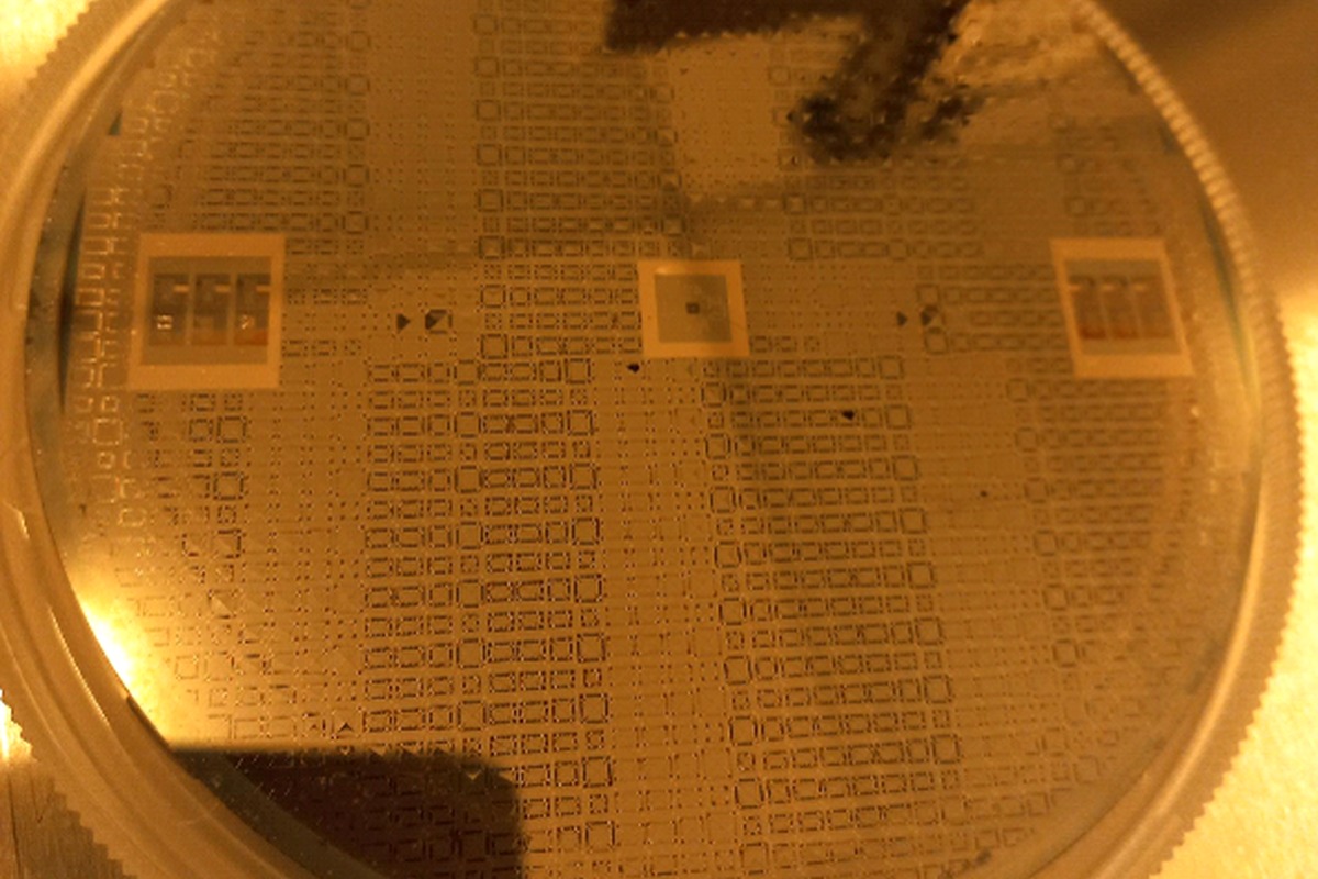
Clear sound, wide bandwidth and compact piezoelectric acoustic devices.
View Platform →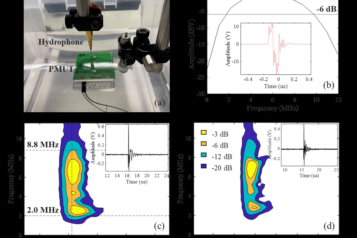
Fast, precise beam steering and optical scanning with low-voltage piezoelectric actuation.
View Platform →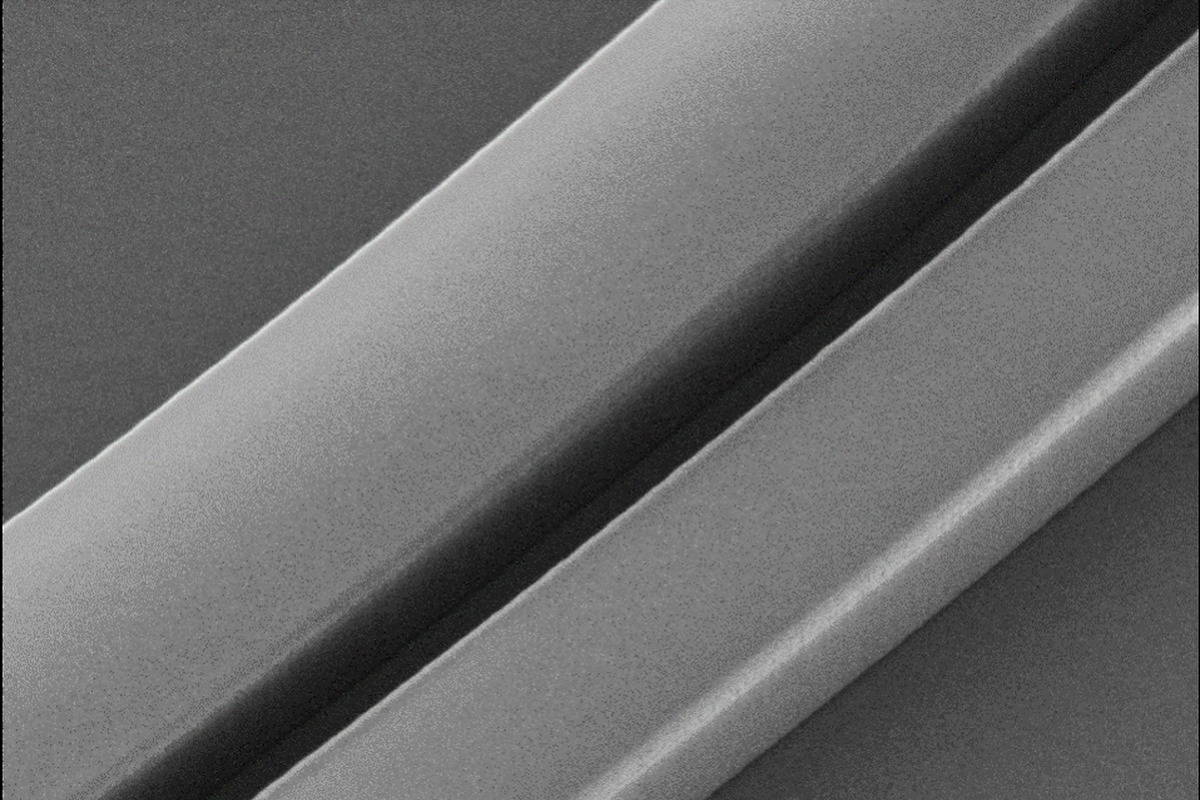
Rugged semiconductor and MEMS platforms for high-power, harsh-environment and advanced sensing applications.
View Platform →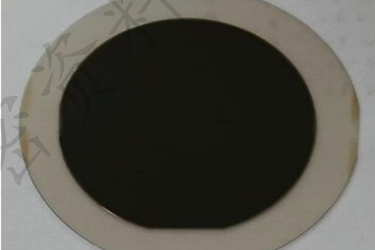
High-speed photonic and optoelectronic platforms for communication, sensing and integrated light sources.
View Platform →
Advanced III–V materials for infrared detection, sensing and integrated optoelectronics.
View Platform →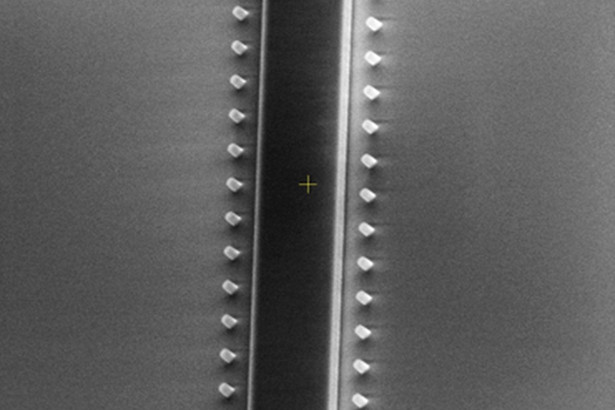
Integrated photonic circuits and wafer-level manufacturing for scalable optical systems.
View Platform →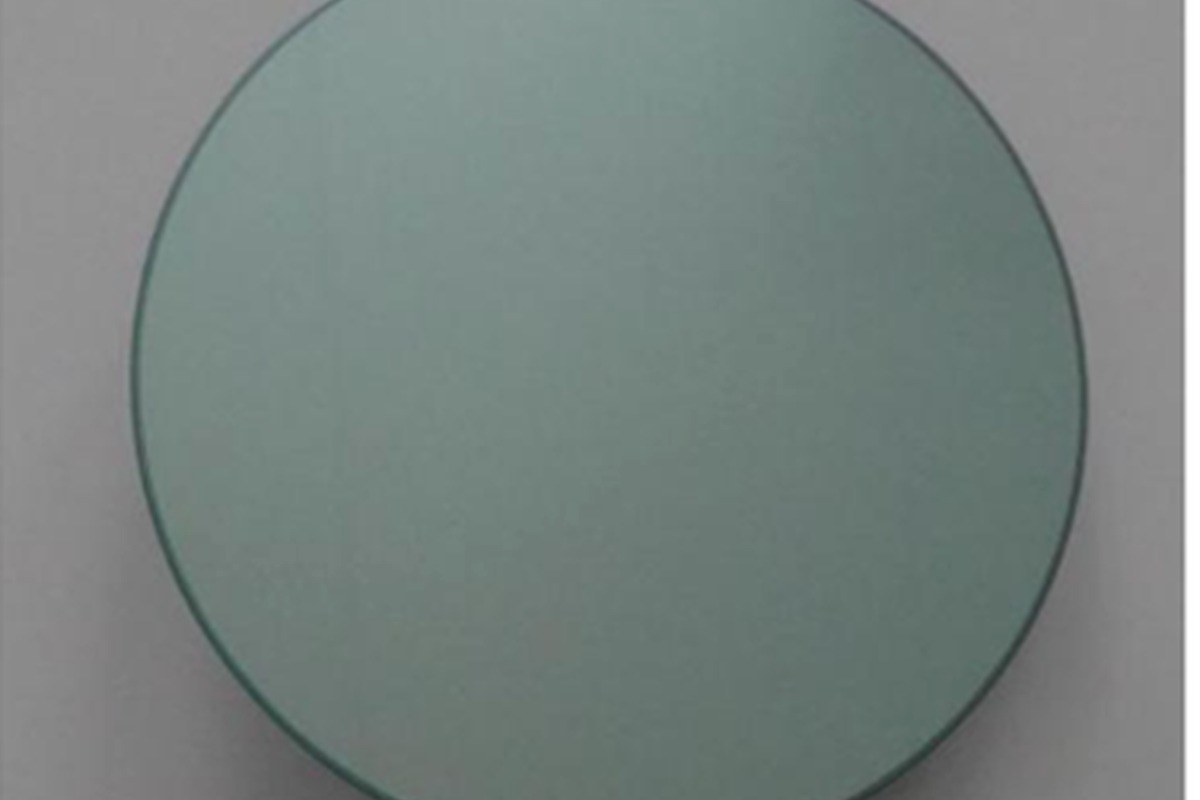
Integrated photonics combined with piezoelectric and BTO-based functional materials for tunable optical devices, high-speed modulation and heterogeneous integration.
View Platform →
GaN-based and advanced custom semiconductor platforms for metasurfaces, photonics, sensing and project-specific integration.
View Platform →From specification and feasibility review to a manufacturable design.
Rapid prototypes and engineering wafers for validation.
Advanced MEMS, photonics and piezoelectric process integration.
Flexible shared-wafer and customer-dedicated manufacturing.
Repeatable wafer-level manufacturing with controlled quality.
Engineering in Switzerland with disciplined documentation and quality control.
Access to specialist semiconductor, photonic and piezoelectric platforms.
A route from engineering devices to 8-inch production.
Customer files, designs and IP are handled under strict confidentiality.
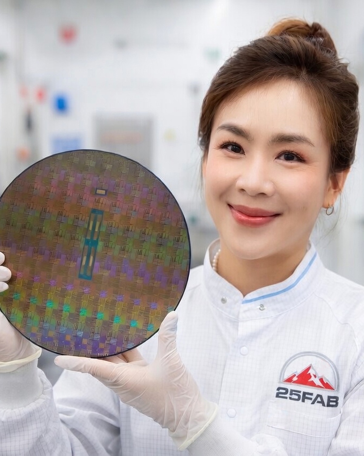
Real wafers, real packaged devices and real fabrication detail — presented with the clarity expected by serious B2B customers.
Authentic fabricated wafers presented with clean, professional visual treatment.
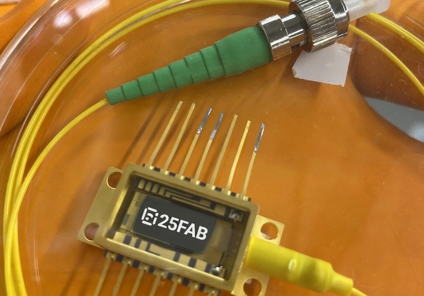
Actual packaged components and device-level engineering, suitable for customer-facing presentation.
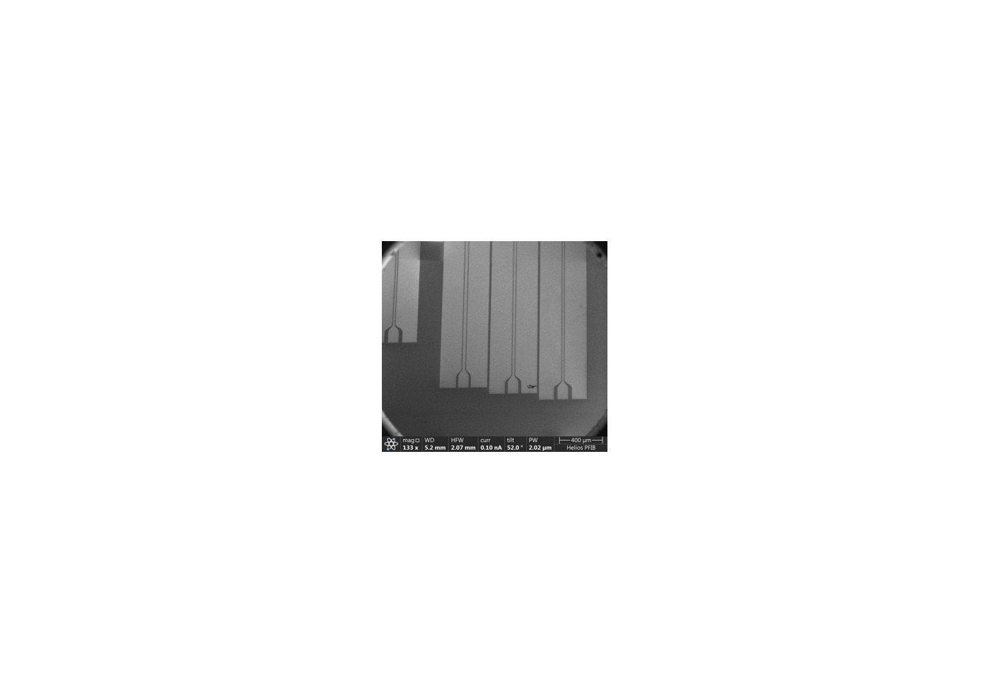
SEM-level device evidence that reinforces process capability and design precision.
25FAB presents real fabrication imagery because high-level customers and partners respond best to concrete engineering proof, not generic visual effects.
The website now combines real engineering imagery with concise commercial messaging to build immediate credibility.
High-end customers do not respond to generic stock imagery. They respond to credible wafer photographs, packaged devices, clean process evidence and a calm, premium visual presentation. This section helps turn technical credibility into commercial confidence.
From engineering samples to wafer-scale production.