Custom wafer development · Dedicated runs · Scale-up

SiC Platforms

Custom silicon-carbide device and process platforms for photonics, MEMS, sensing, power electronics and demanding operating environments.

Rugged semiconductor and MEMS platforms for high-power, harsh-environment and advanced sensing applications.

Harsh-environment capability
High thermal and mechanical stability
Custom wafer and device processing
Engineering samples to repeat production
SiC Platforms

What We Supply

  • SiC wafers and device structures
  • Custom etch and metallisation processes
  • MEMS and photonic structures
  • Diced chips and full-wafer delivery
  • Engineering wafers and pilot lots
  • Metrology and inspection options

Configurable Parameters

  • SiC polytype and wafer type
  • Device-layer thickness
  • Critical dimensions
  • Etch depth and profile
  • Metallisation and contacts
  • Wafer size and quantity

Application Areas

  • Power and RF devices
  • Harsh-environment sensors
  • High-temperature MEMS
  • Photonics and quantum devices
  • Industrial inspection
  • Advanced research platforms

Manufacturing Route

1

Engineering Samples

2

Pilot Production

3

Volume Production

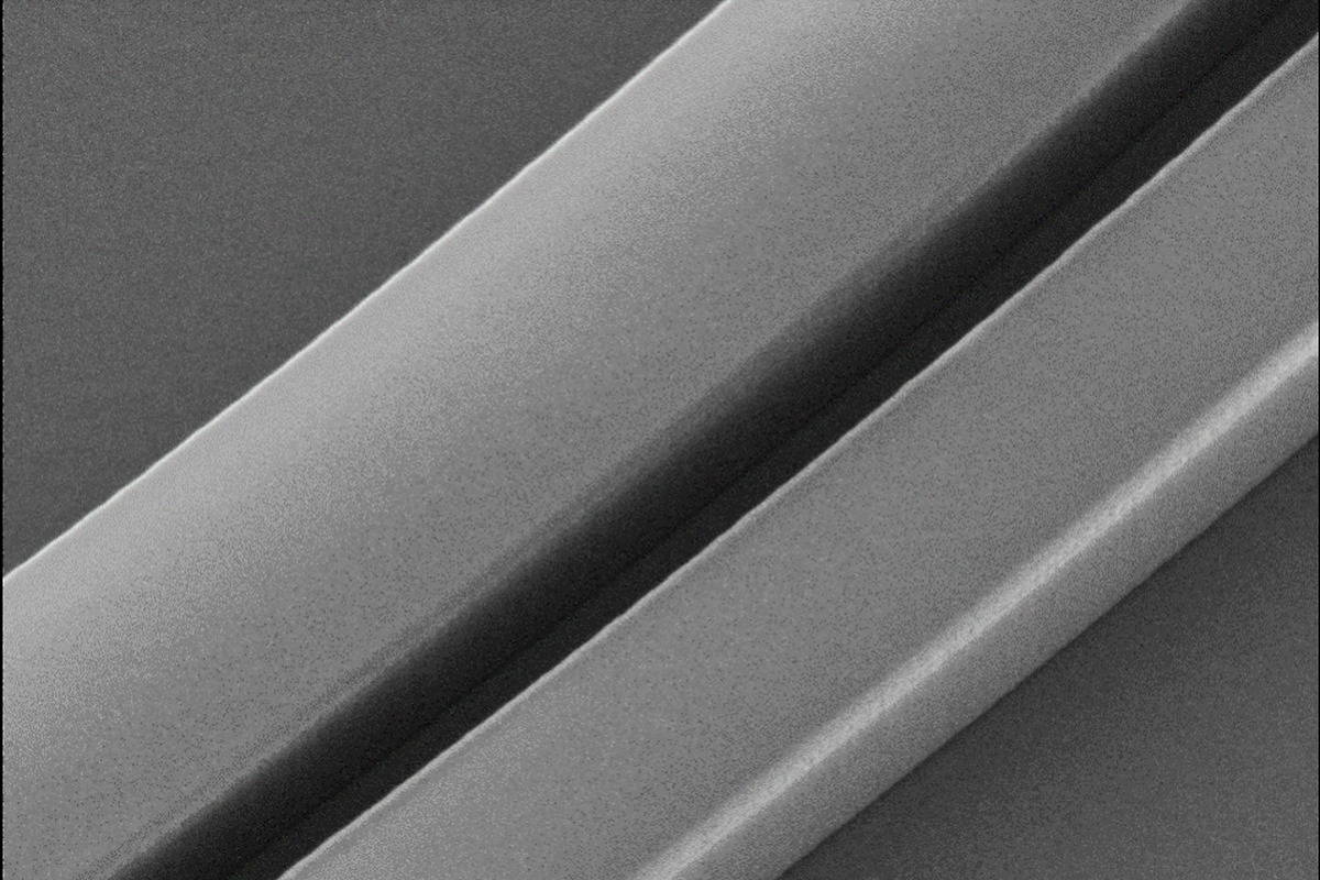
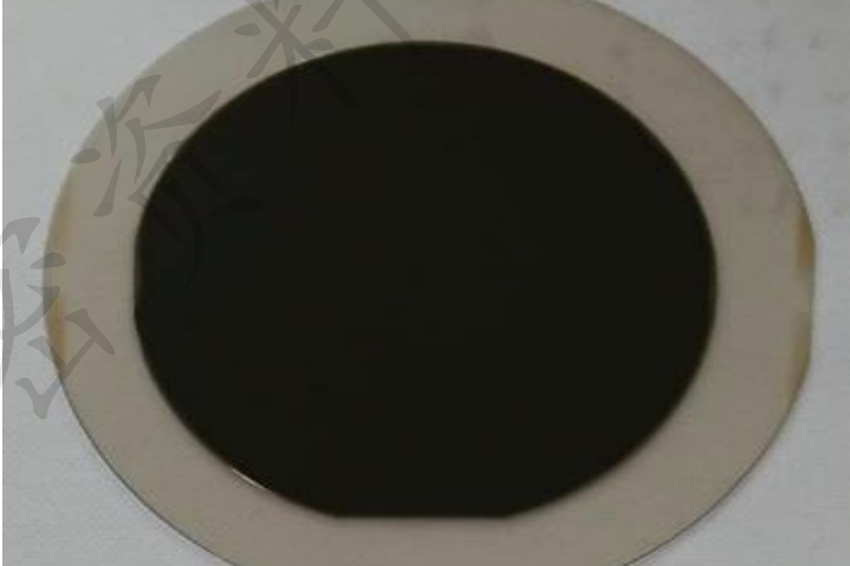
Real Fabrication & Characterisation

Selected 25FAB and project fabrication images presented in a more commercial, customer-ready format.

Contact

SiC Platforms