PMUT · 126% MEASURED BANDWIDTH
PMUT OEM Module
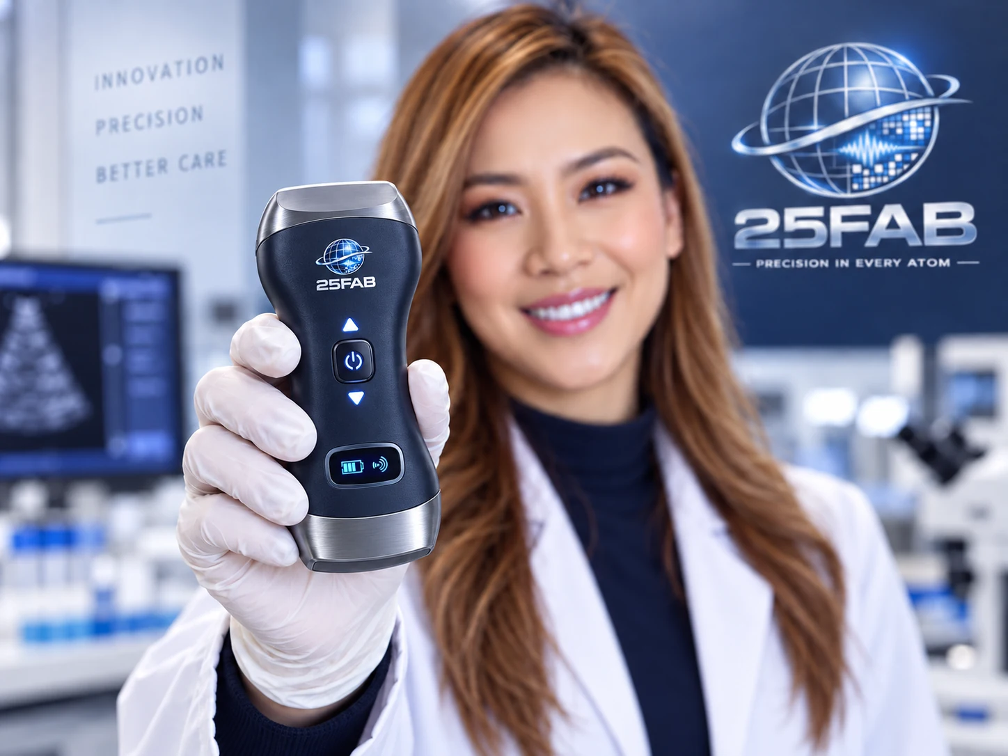
Broadband piezoelectric ultrasound from custom array design to packaged OEM integration. 126% measured bandwidth on the demonstrated platform.
Explore module →25FAB는 디바이스 물리, 형상, 소재 스택과 공정 제약을 AI로 공동 최적화하고 여러 기능성 소재를 웨이퍼 레벨에서 통합합니다. AI 아키텍처부터 실측 engineering wafer, pilot 및 반복 양산까지 지원합니다.
Broadband piezoelectric ultrasound from custom array design to packaged OEM integration. 126% measured bandwidth on the demonstrated platform.
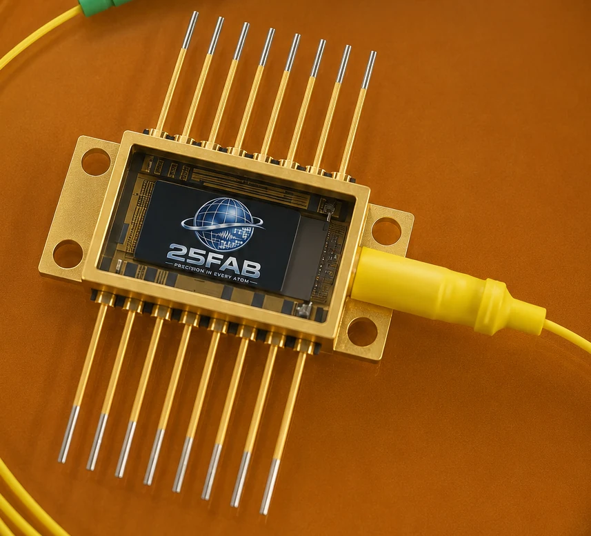
Integrated photonics with piezoelectric actuation, measured 20 MHz/V DC tuning near 1550 nm, and a route from die to packaged module.
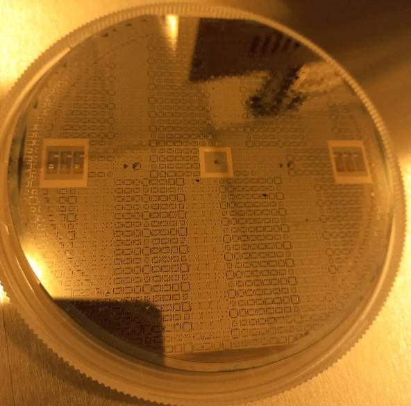
Wafer-level piezoelectric MEMS speaker with 69 dB measured acoustic output, available for custom, pilot and volume manufacturing programs.
Start with measured products. 25FAB puts PMUT, piezo-tunable PICs and the 69 dB piezo MEMS speaker first, with a dedicated module route for quantum systems.
Broadband piezoelectric ultrasound from custom array design to packaged OEM integration. 126% measured bandwidth on the demonstrated platform.
Explore module →Integrated photonics with piezoelectric actuation, measured 20 MHz/V DC tuning near 1550 nm, and a route from die to packaged module.
Explore module →Wafer-level piezoelectric MEMS speaker with 69 dB measured acoustic output, available for custom, pilot and volume manufacturing programs.
Explore module →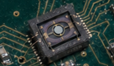
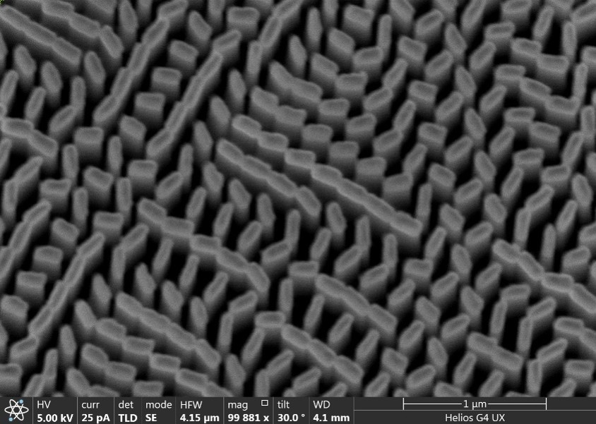
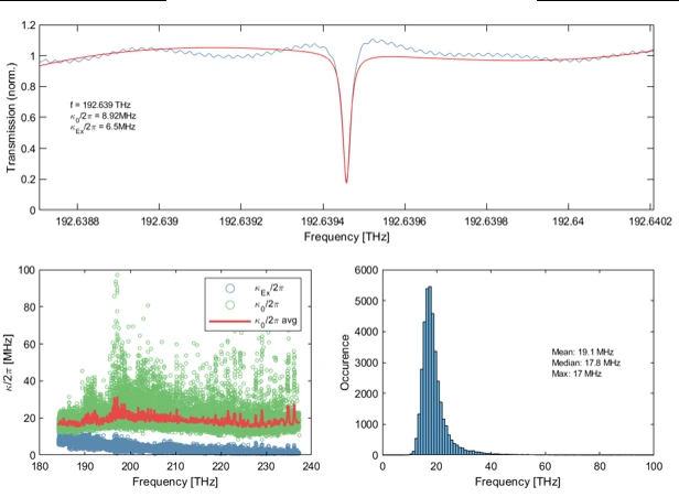
A modular wafer-level route for neutral-atom optical control, quantum photonics and precision beam systems: piezo MEMS, metasurfaces and tunable PICs.
Explore quantum systems →시뮬레이션만이 아니라 AI 설계, 웨이퍼 제조, 측정과 양산을 하나의 폐루프로 연결합니다.
광대역 압전 초음파 플랫폼 · custom, pilot, volume 프로그램.
웨이퍼 레벨 압전 MEMS 스피커 · custom, pilot, volume 생산.
1550 nm 부근 압전 가변 PIC · +10 V / −10 V에서 반복 가능한 응답.
선정 프로그램: design freeze → wafer → 측정 → feedback 약 3개월.
광대역 압전 초음파 플랫폼 · custom, pilot, volume 프로그램.
PILOT + VOLUME 프로그램웨이퍼 레벨 압전 MEMS 스피커 · custom, pilot, volume 생산.
PILOT + VOLUME 프로그램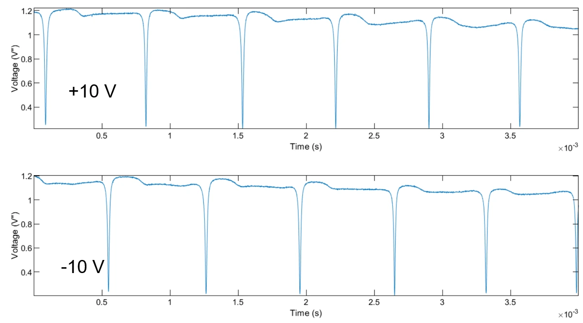
1550 nm 부근 압전 가변 PIC · +10 V / −10 V에서 반복 가능한 응답.
PILOT + VOLUME 프로그램MEMS, 포토닉스, 메타표면, 화합물 반도체 또는 맞춤 디바이스의 기능 목표를 제조 가능한 구조와 다중소재 통합 경로로 변환합니다.
25FAB은 압전, 포토닉, III–V, 와이드밴드갭 및 이종 소재 시스템의 맞춤 설계와 웨이퍼 공정을 지원합니다.
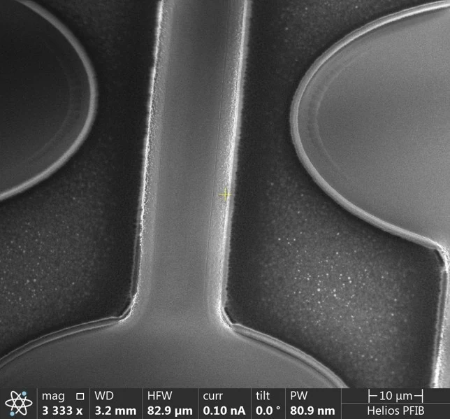
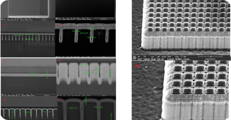
MEMS, 포토닉스, 메타표면, 화합물 반도체 및 맞춤 디바이스 개발과 제조.
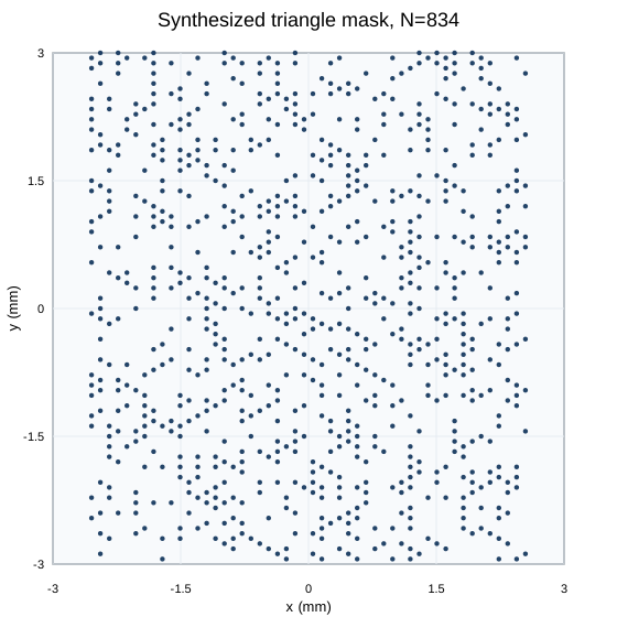
Industrial PMUT chips and arrays aligned to 1–5, 2–6, 3–10, 4–13, 5–15, 8–20 and 1–15 MHz OEM architectures.
플랫폼 보기 →
Clear sound, wide bandwidth and compact piezoelectric acoustic devices.
플랫폼 보기 →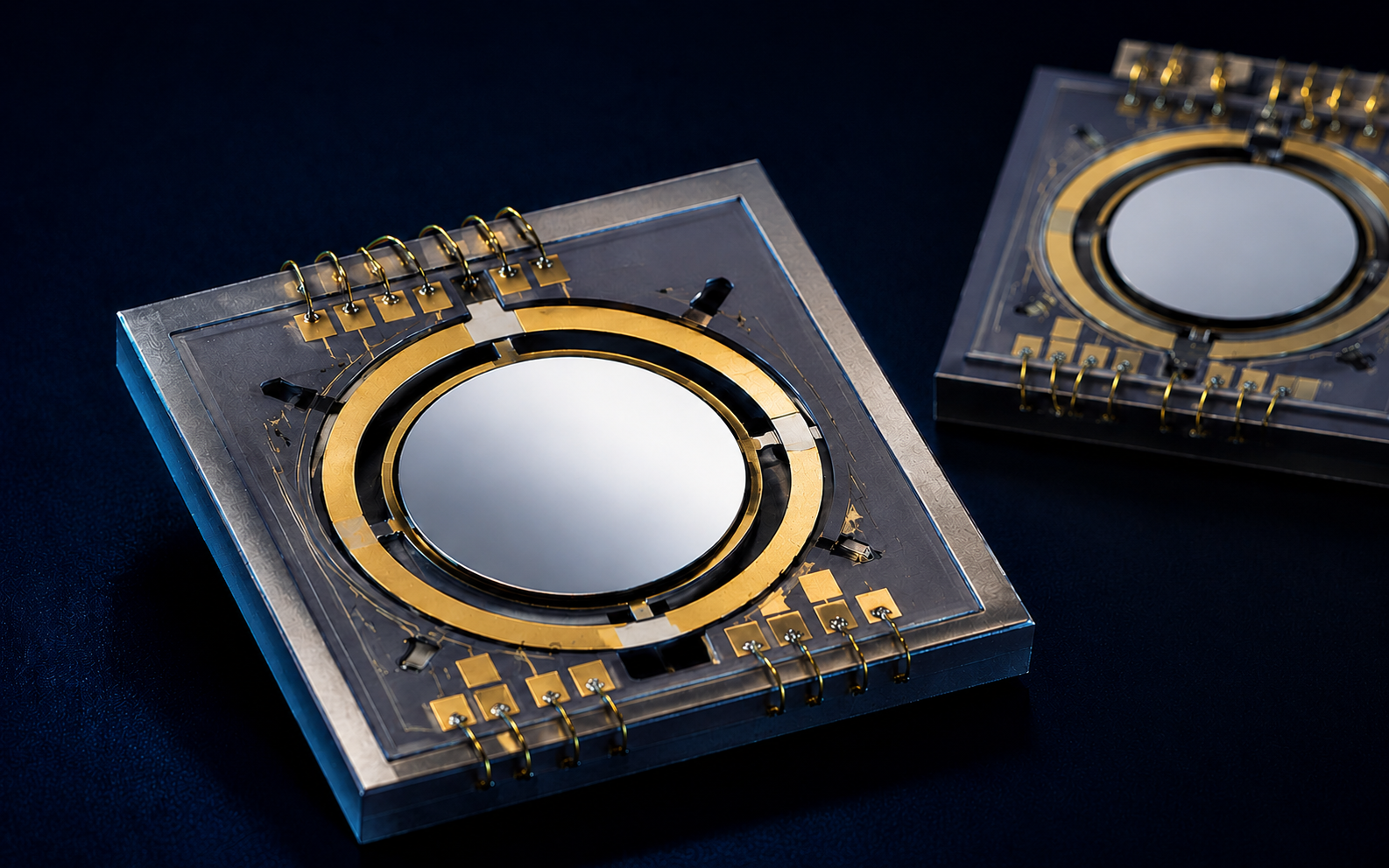
Fast, precise beam steering and optical scanning with low-voltage piezoelectric actuation.
플랫폼 보기 →
Rugged semiconductor and MEMS platforms for high-power, harsh-environment and advanced sensing applications.
플랫폼 보기 →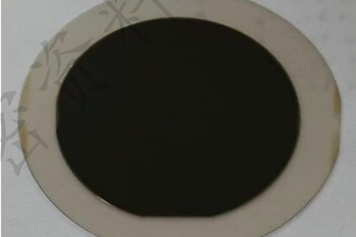
High-speed photonic and optoelectronic platforms for communication, sensing and integrated light sources.
플랫폼 보기 →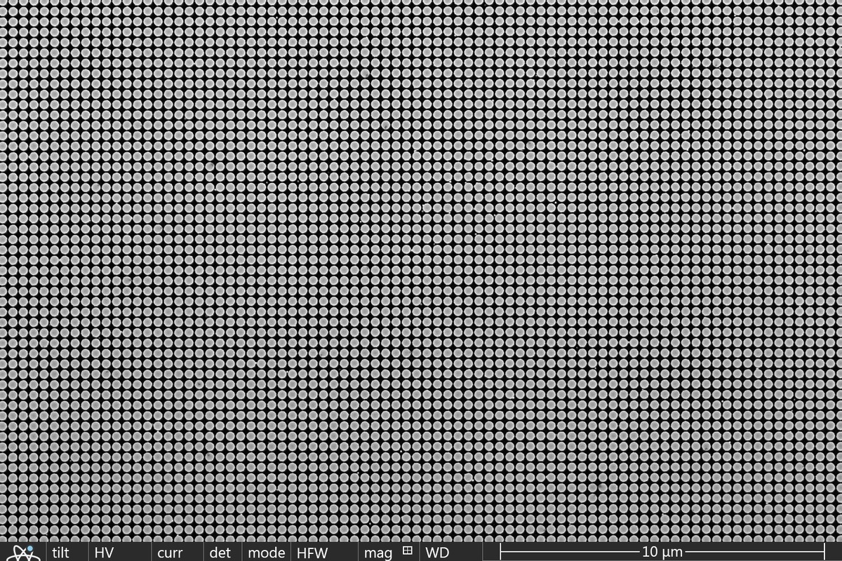
Advanced III–V materials for infrared detection, sensing and integrated optoelectronics.
플랫폼 보기 →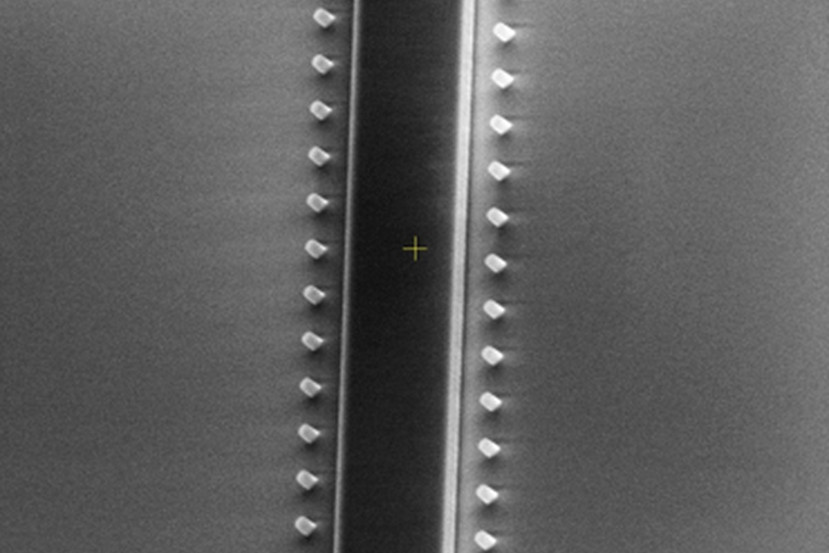
Integrated photonic circuits and wafer-level manufacturing for scalable optical systems.
플랫폼 보기 →
PIC integration with PZT, AlN, AlScN, BTO-on-Si and other electro-optic / piezoelectric functional films.
플랫폼 보기 →
Custom flat-optics, metalens and metasurface devices for beam shaping, focusing, sensing and 3D imaging.
플랫폼 보기 →
Project-specific semiconductor and heterogeneous-integration routes for GaN, GaAs, Ge-on-Si, GeSn, diamond and non-standard material stacks.
플랫폼 보기 →지원 플랫폼은 NRE, engineering wafer, pilot, qualification 및 반복 생산으로 확장할 수 있습니다.
AI 설계 → 다중소재 통합 → engineering wafer → 실측 → pilot → volume
OEM, 연구팀 및 딥테크 기업을 위한 명확한 프로젝트 단계.
Target function, frequency, aperture, geometry, interfaces and delivery format.
Device architecture and process route are aligned with the target application.
Engineering samples or wafers provide the first physical validation point.
Pilot and dedicated wafer routes support the transition toward repeatable supply.
AI 공동설계, 다중소재 모놀리식 통합, 실측 성능, engineering wafer에서 pilot 및 volume production까지.