PMUT · 126% MEASURED BANDWIDTH
PMUT OEM Module
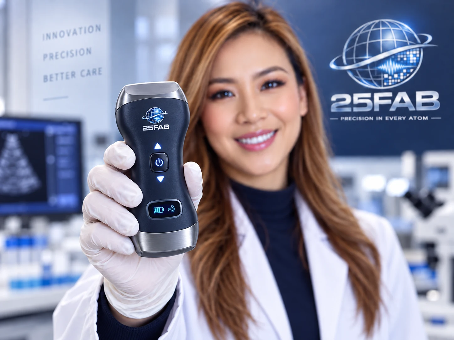
Broadband piezoelectric ultrasound from custom array design to packaged OEM integration. 126% measured bandwidth on the demonstrated platform.
Explore module →25FAB mengoptimumkan bersama fizik peranti, geometri, bahan dan kekangan proses, mengintegrasikan bahan fungsi pada tahap wafer dan membawa program daripada seni bina AI kepada engineering wafer yang diukur, pilot dan pengeluaran berulang.
Broadband piezoelectric ultrasound from custom array design to packaged OEM integration. 126% measured bandwidth on the demonstrated platform.
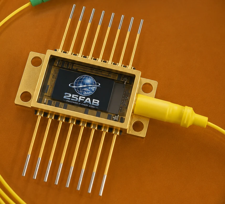
Integrated photonics with piezoelectric actuation, measured 20 MHz/V DC tuning near 1550 nm, and a route from die to packaged module.
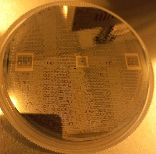
Wafer-level piezoelectric MEMS speaker with 69 dB measured acoustic output, available for custom, pilot and volume manufacturing programs.
Start with measured products. 25FAB puts PMUT, piezo-tunable PICs and the 69 dB piezo MEMS speaker first, with a dedicated module route for quantum systems.
Broadband piezoelectric ultrasound from custom array design to packaged OEM integration. 126% measured bandwidth on the demonstrated platform.
Explore module →Integrated photonics with piezoelectric actuation, measured 20 MHz/V DC tuning near 1550 nm, and a route from die to packaged module.
Explore module →Wafer-level piezoelectric MEMS speaker with 69 dB measured acoustic output, available for custom, pilot and volume manufacturing programs.
Explore module →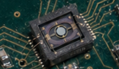
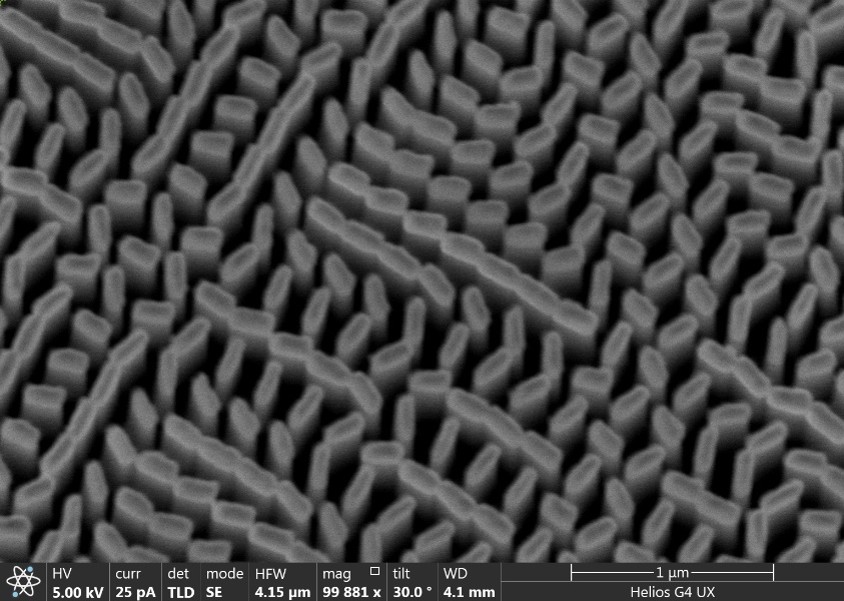
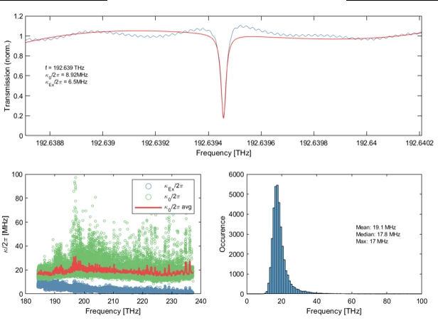
A modular wafer-level route for neutral-atom optical control, quantum photonics and precision beam systems: piezo MEMS, metasurfaces and tunable PICs.
Explore quantum systems →Bukan simulasi sahaja: AI design, wafer fabrication, measurement dan scale-up dalam satu gelung.
Platform ultrasound piezo broadband · custom, pilot, volume.
Speaker Piezo MEMS wafer-level · custom, pilot, volume.
PIC piezo-tunable sekitar 1550 nm · respons berulang pada +10 V / −10 V.
Program terpilih: design freeze → wafer → measurement → feedback.
Platform ultrasound piezo broadband · custom, pilot, volume.
PILOT + VOLUMESpeaker Piezo MEMS wafer-level · custom, pilot, volume.
PILOT + VOLUME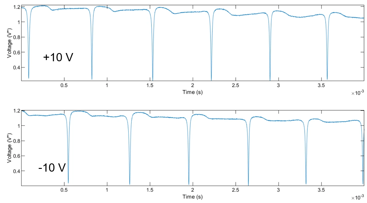
PIC piezo-tunable sekitar 1550 nm · respons berulang pada +10 V / −10 V.
PILOT + VOLUMEHantar sasaran fungsi untuk MEMS, fotonik, metasurface, semikonduktor kompaun atau peranti tersuai untuk diterjemah kepada seni bina boleh dibuat dan laluan integrasi berbilang bahan.
25FAB menyokong reka bentuk dan pemprosesan wafer mengikut projek untuk sistem piezoelektrik, fotonik, III–V, wide-bandgap dan heterogen.
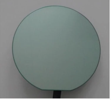
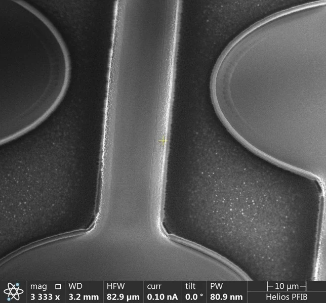
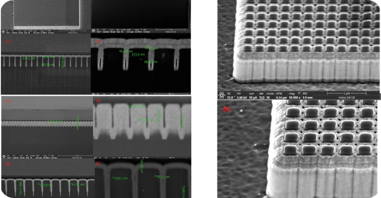
Pembangunan dan pembuatan untuk MEMS, fotonik, metasurface, semikonduktor kompaun dan peranti tersuai.
Industrial PMUT chips and arrays aligned to 1–5, 2–6, 3–10, 4–13, 5–15, 8–20 and 1–15 MHz OEM architectures.
Lihat platform →
Clear sound, wide bandwidth and compact piezoelectric acoustic devices.
Lihat platform →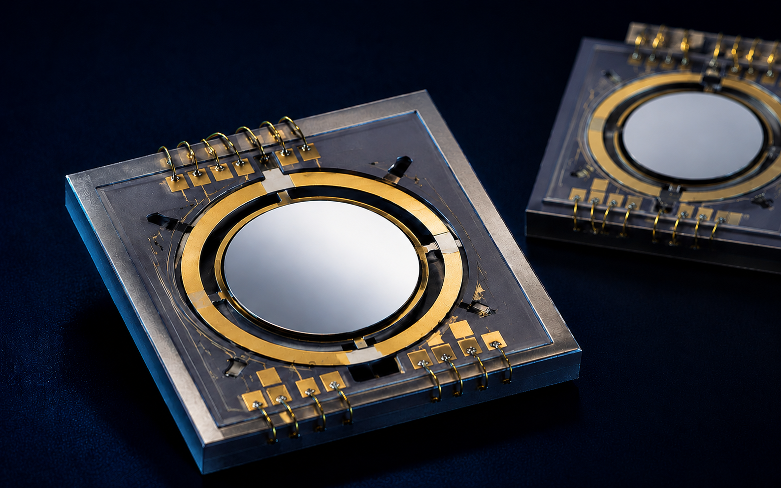
Fast, precise beam steering and optical scanning with low-voltage piezoelectric actuation.
Lihat platform →
Rugged semiconductor and MEMS platforms for high-power, harsh-environment and advanced sensing applications.
Lihat platform →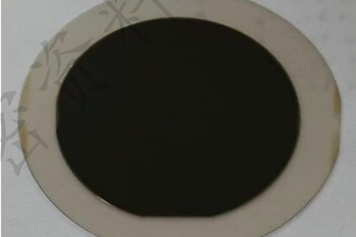
High-speed photonic and optoelectronic platforms for communication, sensing and integrated light sources.
Lihat platform →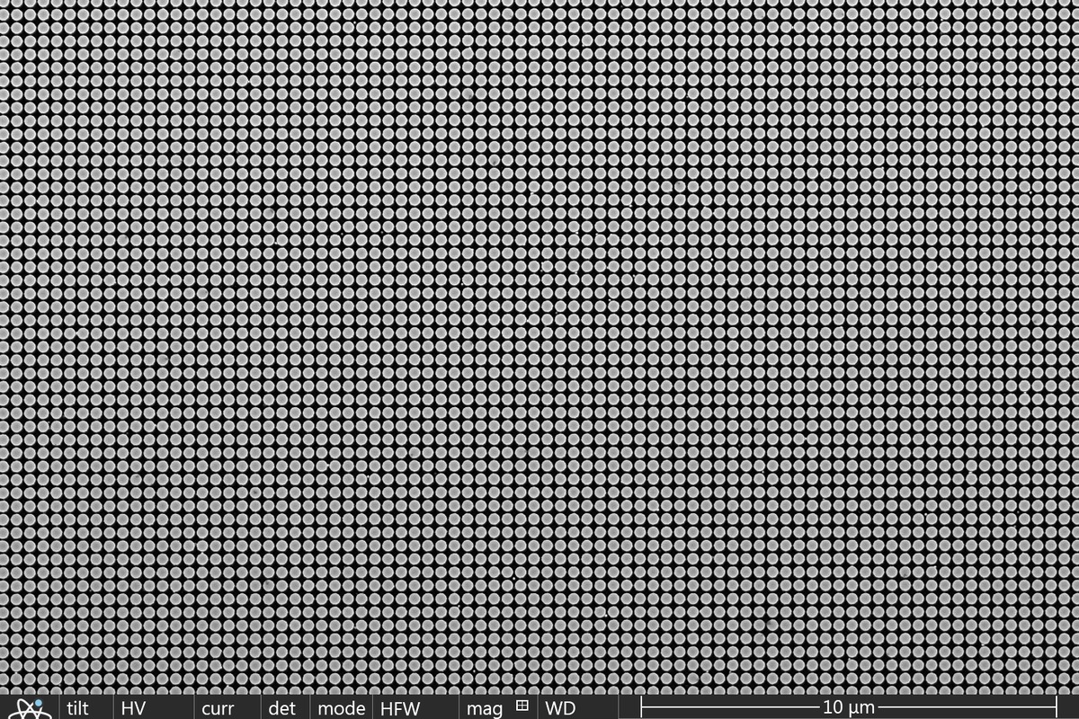
Advanced III–V materials for infrared detection, sensing and integrated optoelectronics.
Lihat platform →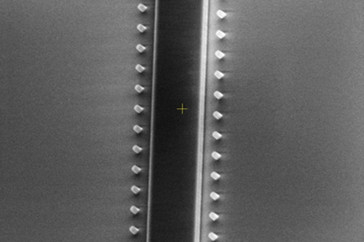
Integrated photonic circuits and wafer-level manufacturing for scalable optical systems.
Lihat platform →
PIC integration with PZT, AlN, AlScN, BTO-on-Si and other electro-optic / piezoelectric functional films.
Lihat platform →
Custom flat-optics, metalens and metasurface devices for beam shaping, focusing, sensing and 3D imaging.
Lihat platform →
Project-specific semiconductor and heterogeneous-integration routes for GaN, GaAs, Ge-on-Si, GeSn, diamond and non-standard material stacks.
Lihat platform →Semua platform disokong boleh bergerak daripada NRE dan engineering wafer ke pilot, qualification dan pengeluaran berulang.
AI design → integrasi multi-material → engineering wafer → measurement → pilot → volume
Fasa projek yang jelas untuk OEM, pasukan penyelidikan dan syarikat deep-tech.
Target function, frequency, aperture, geometry, interfaces and delivery format.
Device architecture and process route are aligned with the target application.
Engineering samples or wafers provide the first physical validation point.
Pilot and dedicated wafer routes support the transition toward repeatable supply.
AI co-design, integrasi monolitik berbilang bahan, prestasi diukur dan laluan daripada engineering wafer ke pilot dan pengeluaran volume.