ENGINEERING · PILOT · VOLUME
PMUT Custom Platforms
Industrial PMUT chips and arrays aligned to 1–5, 2–6, 3–10, 4–13, 5–15, 8–20 and 1–15 MHz OEM architectures.
View Platform →Choose a device or material platform. 25FAB supports AI-assisted design, process integration, engineering wafers, dedicated runs and industrial scale-up.
Industrial PMUT chips and arrays aligned to 1–5, 2–6, 3–10, 4–13, 5–15, 8–20 and 1–15 MHz OEM architectures.
View Platform →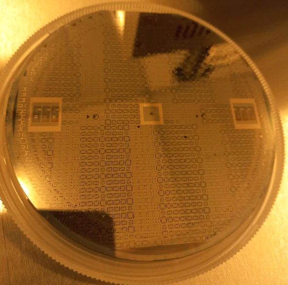
Clear sound, wide bandwidth and compact piezoelectric acoustic devices.
View Platform →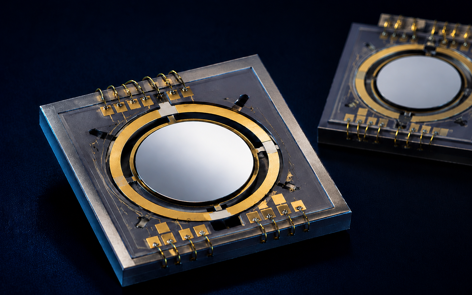
Fast, precise beam steering and optical scanning with low-voltage piezoelectric actuation.
View Platform →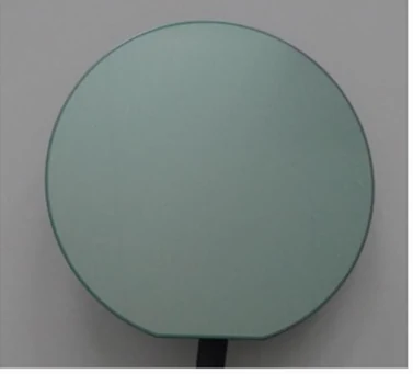
Rugged semiconductor and MEMS platforms for high-power, harsh-environment and advanced sensing applications.
View Platform →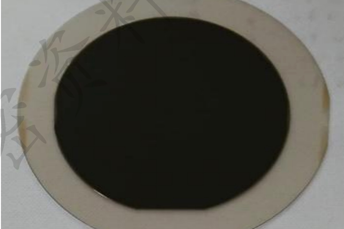
High-speed photonic and optoelectronic platforms for communication, sensing and integrated light sources.
View Platform →
Advanced III–V materials for infrared detection, sensing and integrated optoelectronics.
View Platform →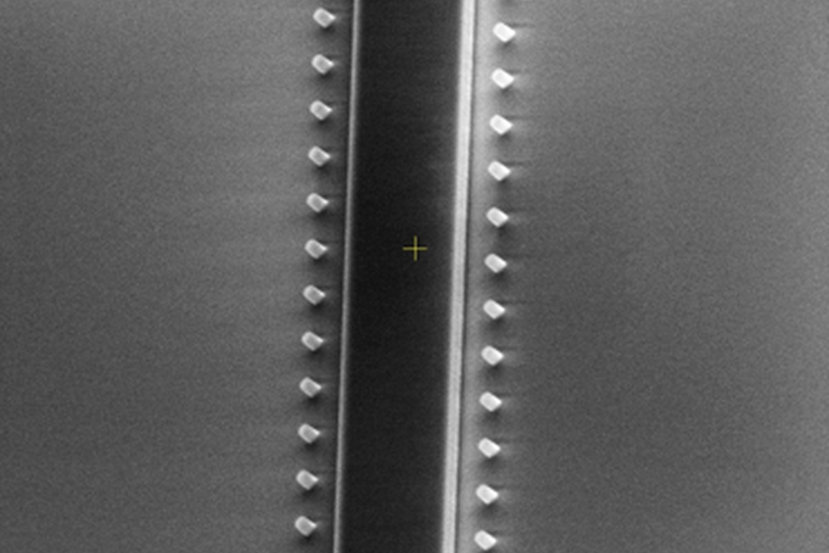
Integrated photonic circuits and wafer-level manufacturing for scalable optical systems.
View Platform →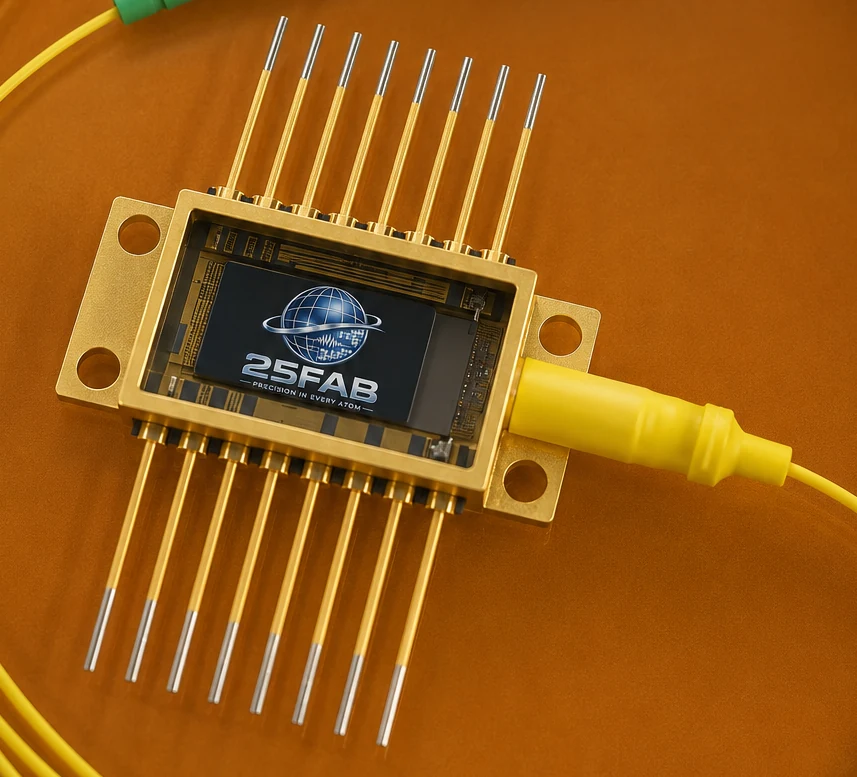
PIC integration with PZT, AlN, AlScN, BTO-on-Si and other electro-optic / piezoelectric functional films.
View Platform →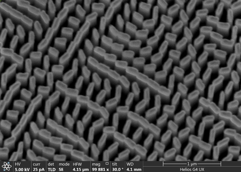
Custom flat-optics, metalens and metasurface devices for beam shaping, focusing, sensing and 3D imaging.
View Platform →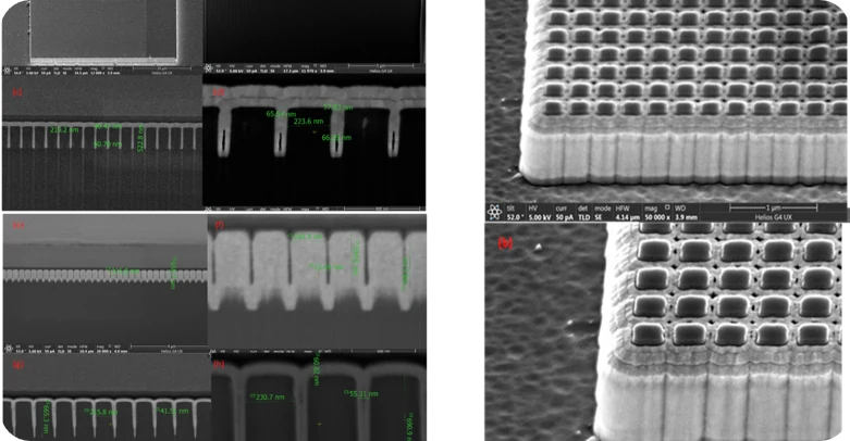
Project-specific semiconductor and heterogeneous-integration routes for GaN, GaAs, Ge-on-Si, GeSn, diamond and non-standard material stacks.
View Platform →25FAB supports project-specific design and wafer processing across piezoelectric, photonic, III–V, wide-bandgap and heterogeneous material systems.
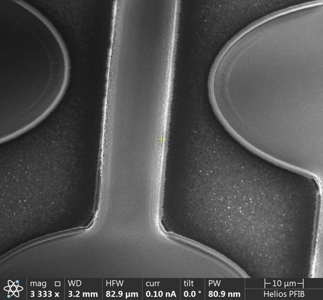
Swiss engineering from AI-assisted device design to wafer-level manufacturing across piezoelectric MEMS, photonics, III–V, wide-bandgap and heterogeneous material systems.