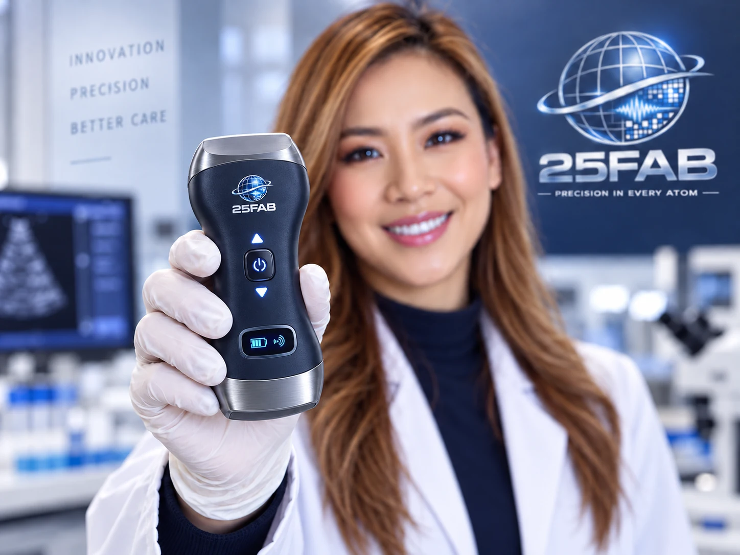
PMUT · 126% MEASURED BANDWIDTH
PMUT OEM Module
Broadband piezoelectric ultrasound from custom array design to packaged OEM integration. 126% measured bandwidth on the demonstrated platform.
Explore module →25FAB 將器件物理、幾何結構、材料堆疊與製程限制一起進行 AI 協同最佳化,並在共同晶圓級平台整合多種功能材料;從 AI 架構、工程晶圓與實測回饋,到試產、qualification 與持續量產供貨。

Broadband piezoelectric ultrasound from custom array design to packaged OEM integration. 126% measured bandwidth on the demonstrated platform.
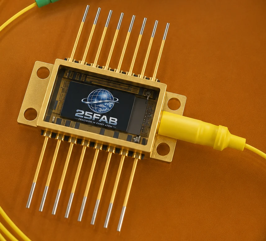
Integrated photonics with piezoelectric actuation, measured 20 MHz/V DC tuning near 1550 nm, and a route from die to packaged module.
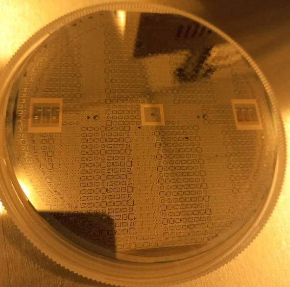
Wafer-level piezoelectric MEMS speaker with 69 dB measured acoustic output, available for custom, pilot and volume manufacturing programs.
Start with measured products. 25FAB puts PMUT, piezo-tunable PICs and the 69 dB piezo MEMS speaker first, with a dedicated module route for quantum systems.
Broadband piezoelectric ultrasound from custom array design to packaged OEM integration. 126% measured bandwidth on the demonstrated platform.
Explore module →Integrated photonics with piezoelectric actuation, measured 20 MHz/V DC tuning near 1550 nm, and a route from die to packaged module.
Explore module →Wafer-level piezoelectric MEMS speaker with 69 dB measured acoustic output, available for custom, pilot and volume manufacturing programs.
Explore module →
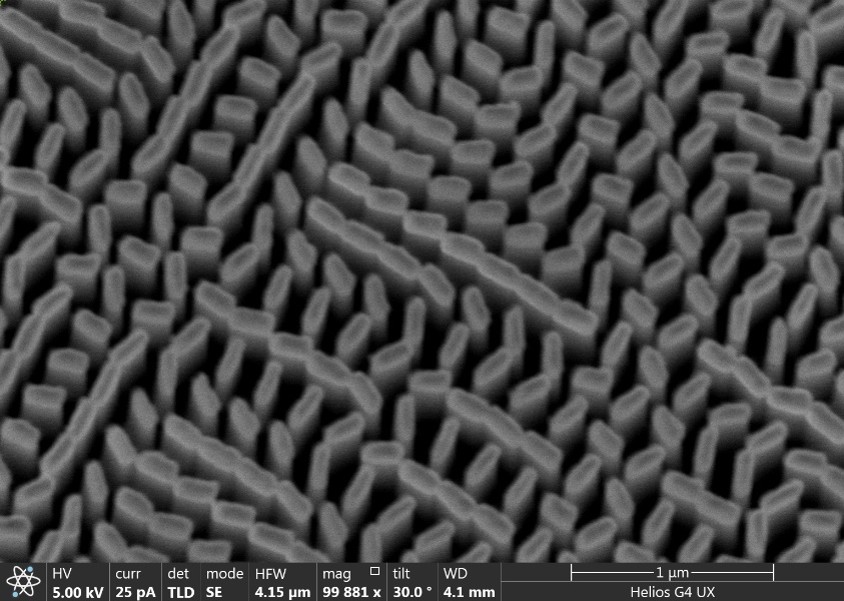
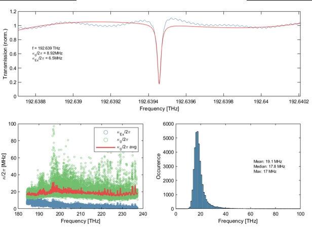
A modular wafer-level route for neutral-atom optical control, quantum photonics and precision beam systems: piezo MEMS, metasurfaces and tunable PICs.
Explore quantum systems →25FAB 將 AI 設計、晶圓製造、器件測試與量產放在同一閉環中。
寬頻壓電超音波平台 · 接受客製、試產與量產專案。
晶圓級壓電 MEMS Speaker · 接受客製、試產與量產。
約 1550 nm 壓電可調 PIC · +10 V / −10 V 下具有可重複光學響應。
部分專案:設計凍結 → 晶圓製造 → 測試 → 設計回饋約 3 個月。
寬頻壓電超音波平台 · 接受客製、試產與量產專案。
接受試產 + 量產晶圓級壓電 MEMS Speaker · 接受客製、試產與量產。
接受試產 + 量產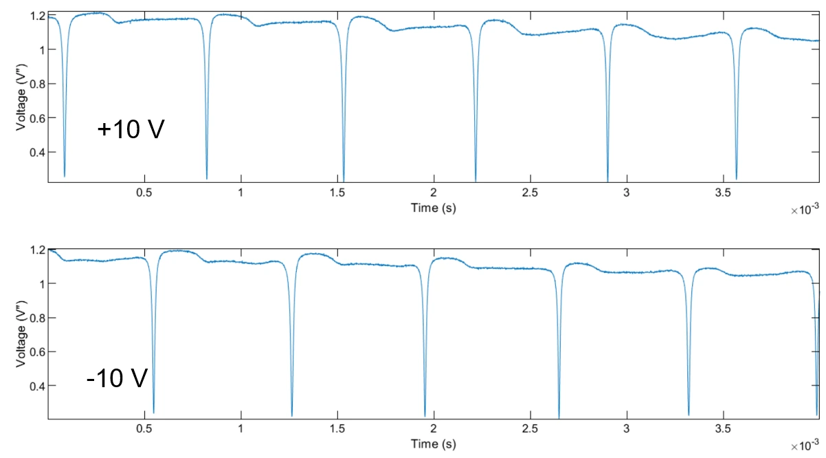
約 1550 nm 壓電可調 PIC · +10 V / −10 V 下具有可重複光學響應。
接受試產 + 量產提交 MEMS、光子、超表面、化合物半導體或客製器件的功能目標,轉換為可製造架構與多材料整合路線。
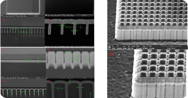
涵蓋 MEMS、光子、超表面、化合物半導體與客製器件的開發與製造。
Industrial PMUT chips and arrays aligned to 1–5, 2–6, 3–10, 4–13, 5–15, 8–20 and 1–15 MHz OEM architectures.
查看平台 →
Clear sound, wide bandwidth and compact piezoelectric acoustic devices.
查看平台 →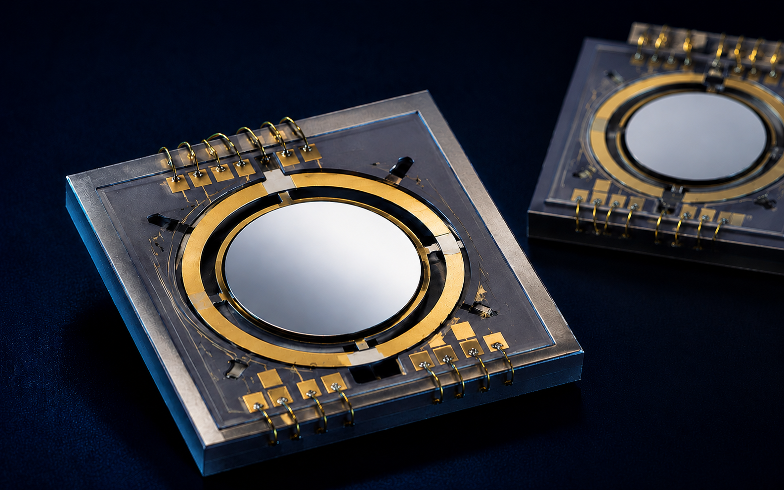
Fast, precise beam steering and optical scanning with low-voltage piezoelectric actuation.
查看平台 →
Rugged semiconductor and MEMS platforms for high-power, harsh-environment and advanced sensing applications.
查看平台 →
High-speed photonic and optoelectronic platforms for communication, sensing and integrated light sources.
查看平台 →
Advanced III–V materials for infrared detection, sensing and integrated optoelectronics.
查看平台 →
Integrated photonic circuits and wafer-level manufacturing for scalable optical systems.
查看平台 →
PIC integration with PZT, AlN, AlScN, BTO-on-Si and other electro-optic / piezoelectric functional films.
查看平台 →
Custom flat-optics, metalens and metasurface devices for beam shaping, focusing, sensing and 3D imaging.
查看平台 →
Project-specific semiconductor and heterogeneous-integration routes for GaN, GaAs, Ge-on-Si, GeSn, diamond and non-standard material stacks.
查看平台 →所有支援平台可由 NRE、工程晶圓推進至試產、qualification 與持續晶圓級量產。
AI 設計 → 多材料單片整合 → 工程晶圓 → 實測驗證 → 試產 → 量產
為 OEM、研究團隊與深科技公司提供清晰專案流程。
Target function, frequency, aperture, geometry, interfaces and delivery format.
Device architecture and process route are aligned with the target application.
Engineering samples or wafers provide the first physical validation point.
Pilot and dedicated wafer routes support the transition toward repeatable supply.