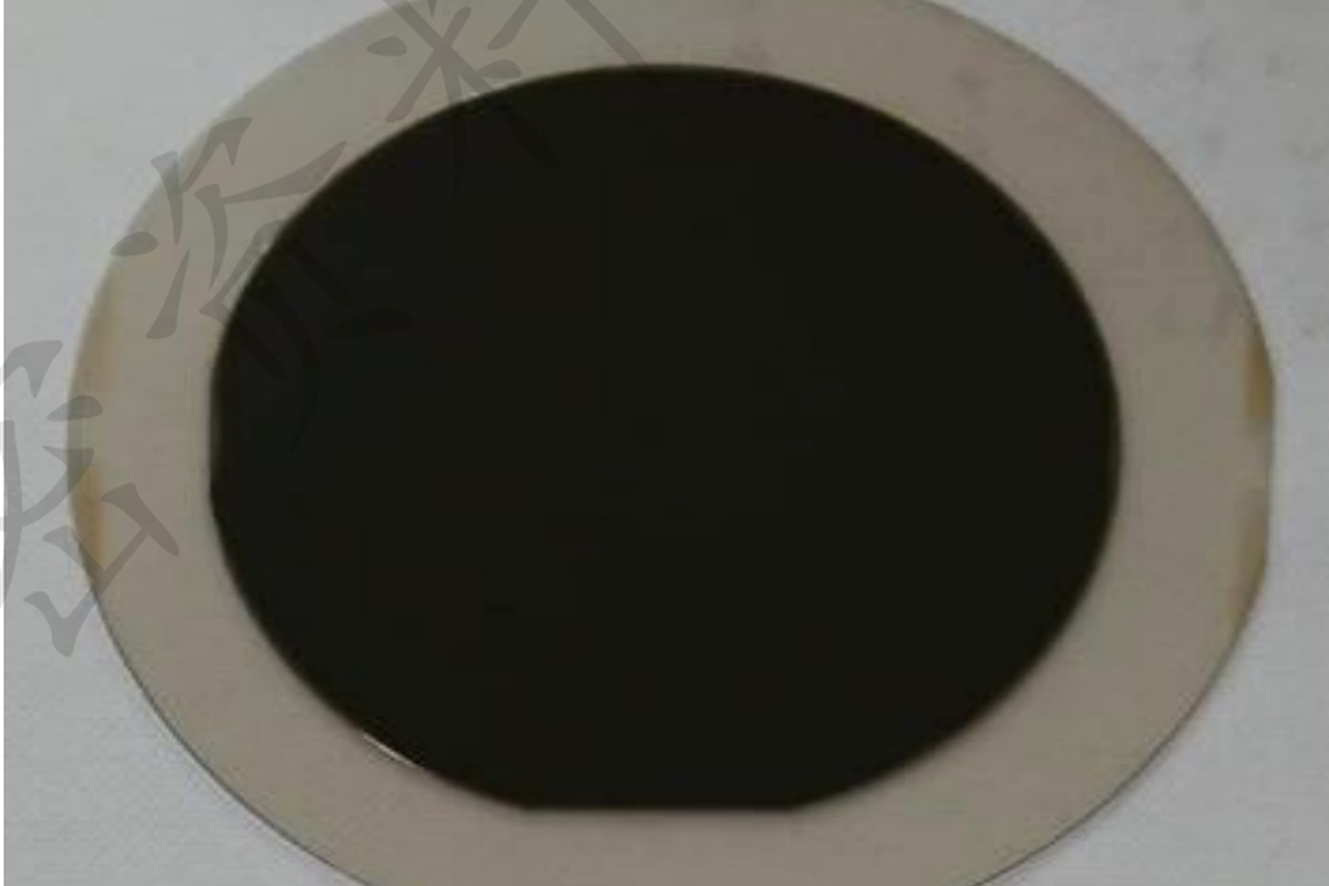
Custom development · Engineering wafers · Dedicated production

InAs / InGaAs平台

Custom InAs and InGaAs device platforms for photodetectors, infrared sensing, high-speed electronics and heterogeneous integration.

面向红外探测、传感与集成光电子的先进III-V平台。

Infrared-sensitive material platforms
Custom III–V process integration
Detector and sensing architectures
Diced chip and wafer-level delivery
InAs / InGaAs平台

交付内容

  • InAs and InGaAs device wafers
  • Photodetector and sensor structures
  • Custom mesa, passivation and contact processes
  • Test chips and engineering wafers
  • Diced components and full-wafer delivery
  • Pilot and recurring production support
可配置参数

  • Epitaxial structure
  • Wavelength or sensing target
  • Device geometry
  • Passivation and contact stack
  • Wafer dimensions
  • Prototype and annual quantity

应用领域

  • Infrared detection
  • Gas and chemical sensing
  • Scientific instrumentation
  • Quantum and cryogenic devices
  • High-speed optoelectronics
  • Integrated sensing systems

制造路线

1

工程样品

2

试产

3

量产

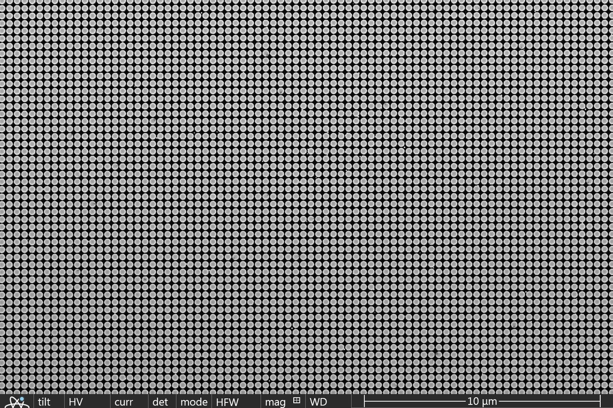
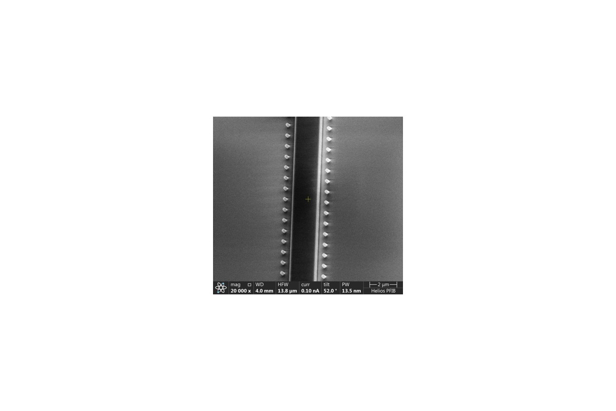
真实制造与表征

精选25FAB及项目相关的真实制造与表征图片,以更适合客户理解和判断的方式呈现。
联系我们

InAs / InGaAs平台