Custom wafer development · Dedicated runs · Scale-up

SiC平台

Custom silicon-carbide device and process platforms for photonics, MEMS, sensing, power electronics and demanding operating environments.

面向高功率、恶劣环境及先进传感的坚固平台。

Harsh-environment capability
High thermal and mechanical stability
Custom wafer and device processing
Engineering samples to repeat production
SiC平台

交付内容

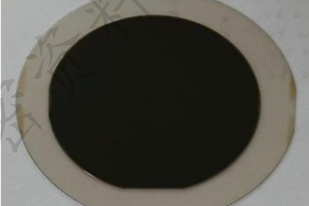
  • SiC wafers and device structures
  • Custom etch and metallisation processes
  • MEMS and photonic structures
  • Diced chips and full-wafer delivery
  • Engineering wafers and pilot lots
  • Metrology and inspection options

可配置参数

  • SiC polytype and wafer type
  • Device-layer thickness
  • Critical dimensions
  • Etch depth and profile
  • Metallisation and contacts
  • Wafer size and quantity

应用领域

  • Power and RF devices
  • Harsh-environment sensors
  • High-temperature MEMS
  • Photonics and quantum devices
  • Industrial inspection
  • Advanced research platforms

制造路线

1

工程样品

2

试产

3

量产

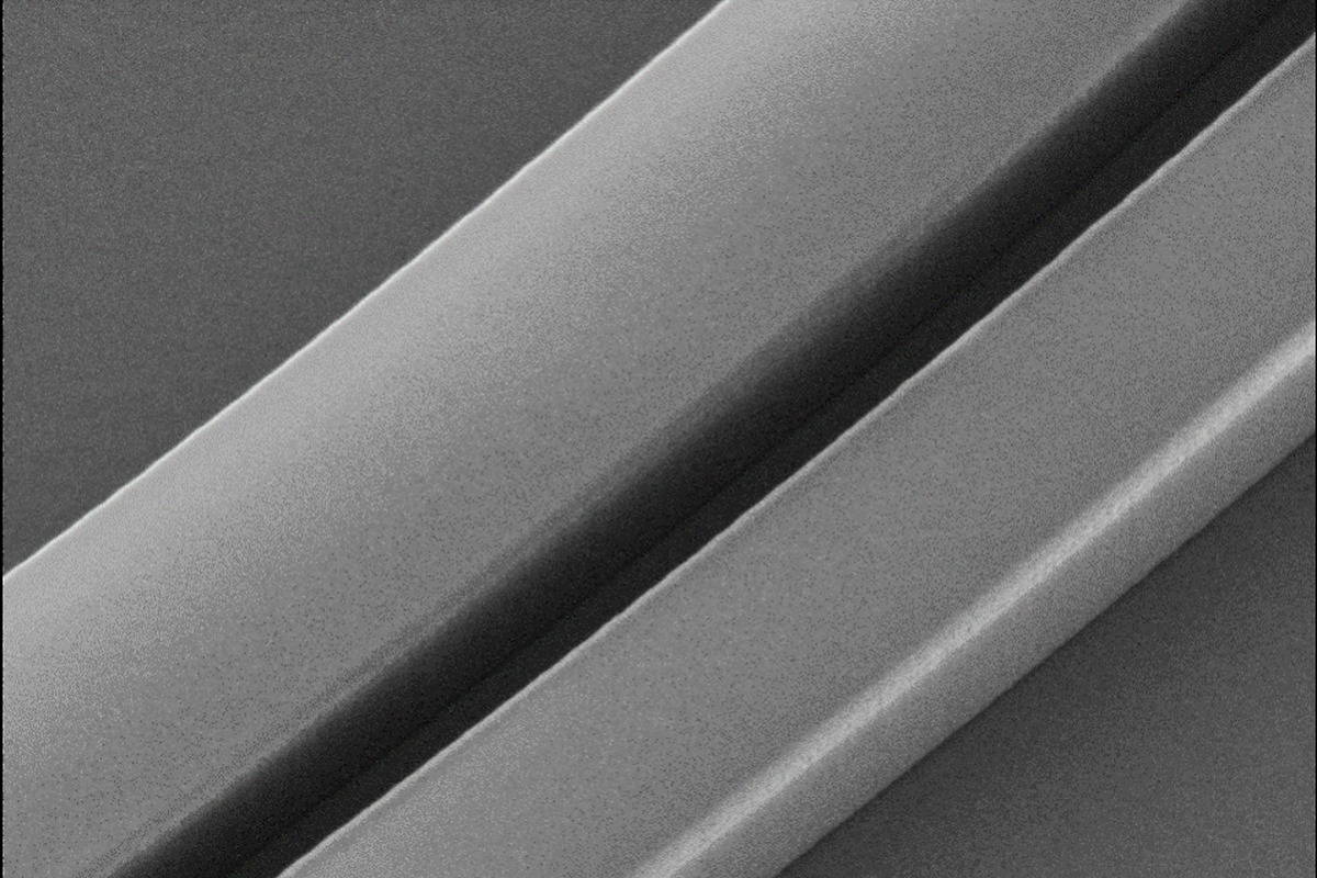
真实制造与表征

精选25FAB及项目相关的真实制造与表征图片,以更适合客户理解和判断的方式呈现。

联系我们

SiC平台