
AI 設計 提交需求
ZH-TW
SPECIALIST TECHNOLOGY PORTFOLIO

核心技術平台

選擇器件或材料平台。25FAB 提供 AI 輔助設計、製程整合、工程晶圓、專用流片與產業級放大量產。

PMUT 客製平台
ENGINEERING · PILOT · VOLUME

PMUT 客製平台

Industrial PMUT chips and arrays aligned to 1–5, 2–6, 3–10, 4–13, 5–15, 8–20 and 1–15 MHz OEM architectures.

查看平台 →
壓電 MEMS 麥克風與微型揚聲器
ENGINEERING · PILOT · VOLUME

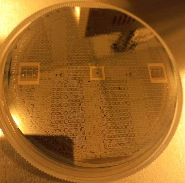
壓電 MEMS 麥克風與微型揚聲器

Clear sound, wide bandwidth and compact piezoelectric acoustic devices.

查看平台 →
壓電 MEMS 微鏡
ENGINEERING · PILOT · VOLUME

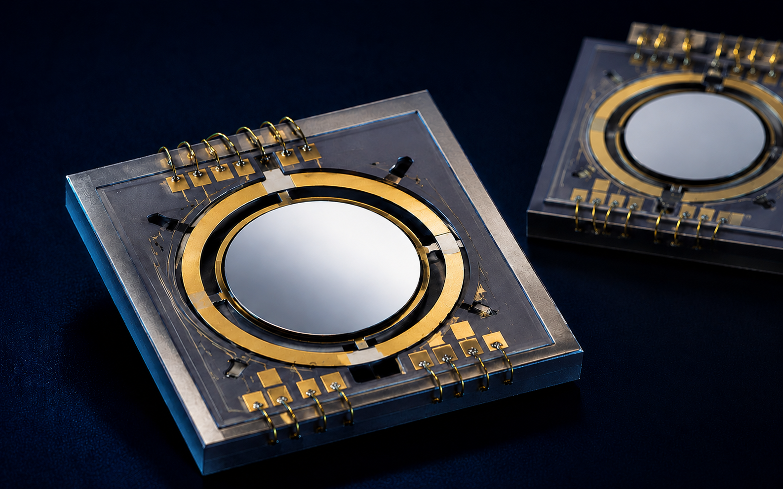
壓電 MEMS 微鏡

Fast, precise beam steering and optical scanning with low-voltage piezoelectric actuation.

查看平台 →
SiC 平台
ENGINEERING · PILOT · VOLUME

SiC 平台

Rugged semiconductor and MEMS platforms for high-power, harsh-environment and advanced sensing applications.

查看平台 →
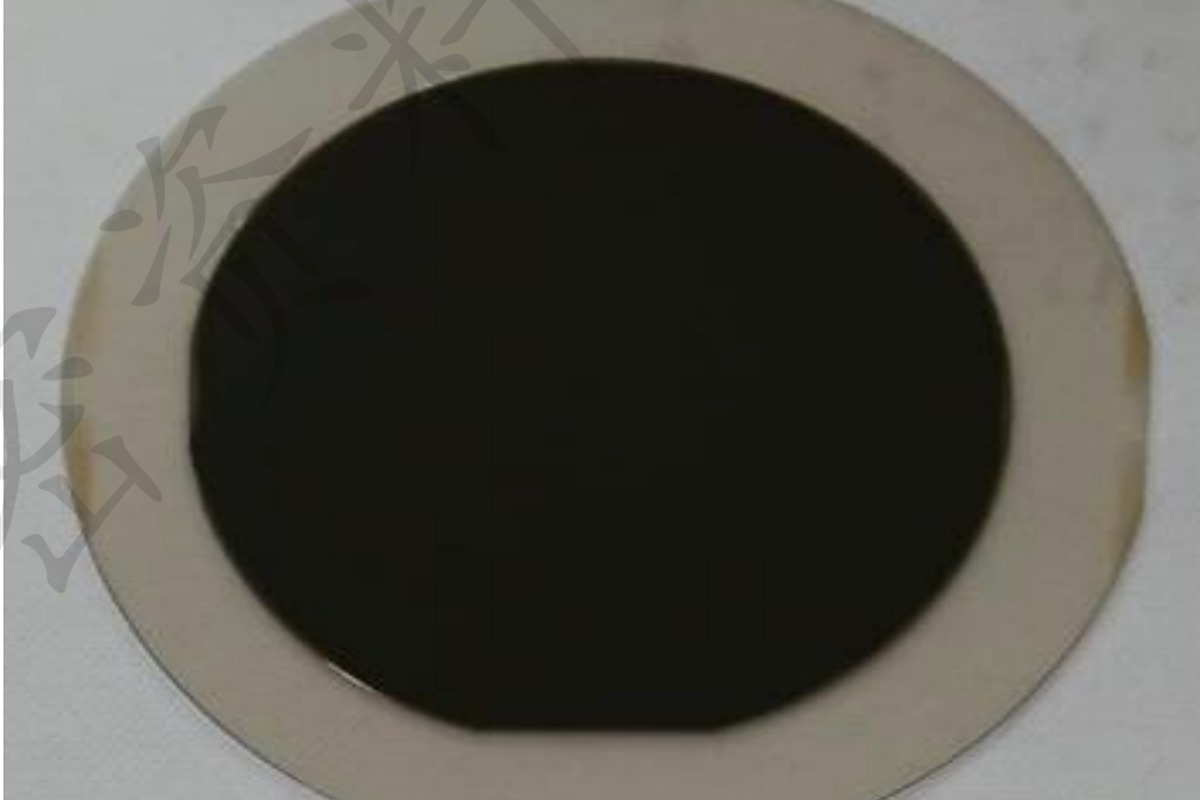
InP 平台
ENGINEERING · PILOT · VOLUME

InP 平台

High-speed photonic and optoelectronic platforms for communication, sensing and integrated light sources.

查看平台 →
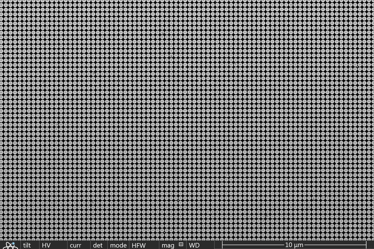
InAs / InGaAs 平台
ENGINEERING · PILOT · VOLUME

InAs / InGaAs 平台

Advanced III–V materials for infrared detection, sensing and integrated optoelectronics.

查看平台 →
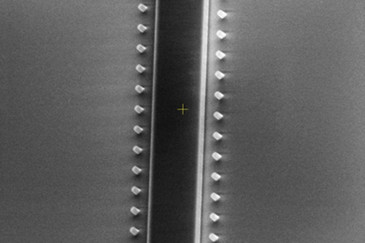
PIC 光子積體平台
ENGINEERING · PILOT · VOLUME

PIC 光子積體平台

Integrated photonic circuits and wafer-level manufacturing for scalable optical systems.

查看平台 →
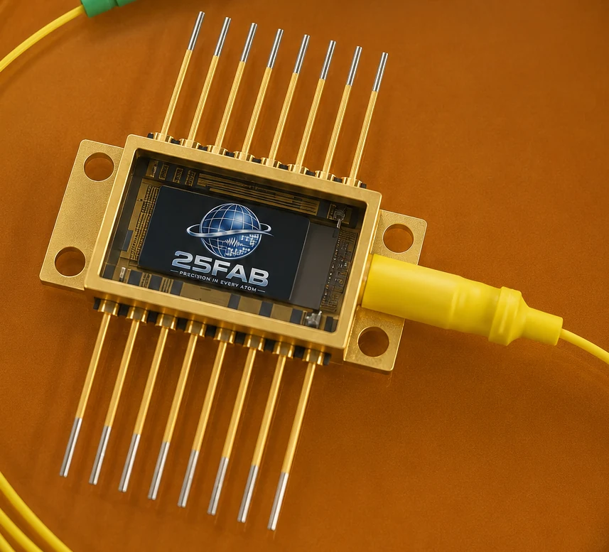
PIC + 壓電 / BTO 整合
ENGINEERING · PILOT · VOLUME

PIC + 壓電 / BTO 整合

PIC integration with PZT, AlN, AlScN, BTO-on-Si and other electro-optic / piezoelectric functional films.

查看平台 →
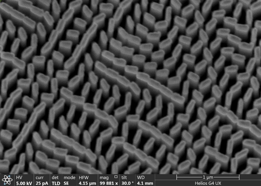
超表面與超透鏡平台
ENGINEERING · PILOT · VOLUME

超表面與超透鏡平台

Custom flat-optics, metalens and metasurface devices for beam shaping, focusing, sensing and 3D imaging.

查看平台 →
GaN、GaAs、GeSn、鑽石與先進客製平台
ENGINEERING · PILOT · VOLUME

GaN、GaAs、GeSn、鑽石與先進客製平台

Project-specific semiconductor and heterogeneous-integration routes for GaN, GaAs, Ge-on-Si, GeSn, diamond and non-standard material stacks.

查看平台 →
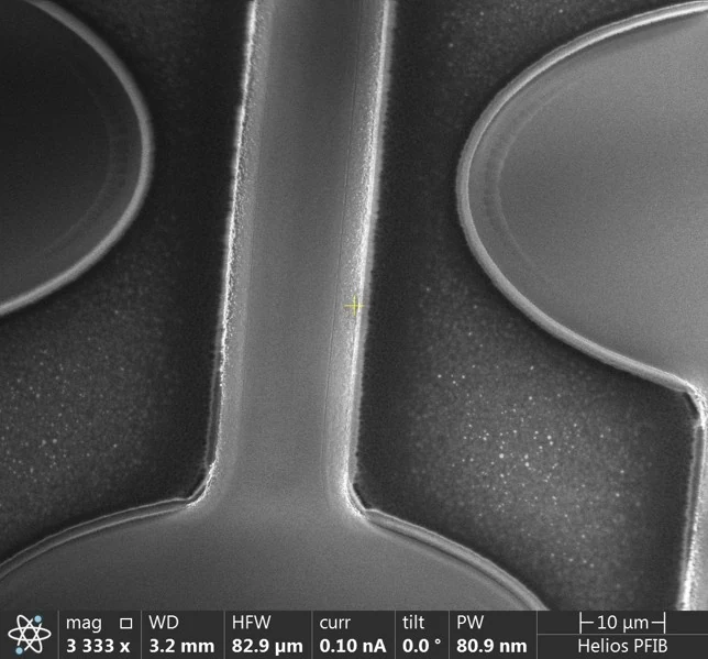
材料與晶圓代工

一個多材料製造入口

25FAB 支援壓電、光子、III–V、寬能隙與異質材料系統的專案設計與晶圓製程。

標準 / 已建立路線

Piezoelectric / electro-optic

PZTAlNAlScN (≤40% Sc)BTO-on-Si
標準 / 已建立路線

Photonics / silicon

Si₃N₄SOIGe-on-SiGeSn
標準 / 已建立路線

III–V semiconductors

GaAsInPInAsInGaAsGaN / AlGaN/GaN
標準 / 已建立路線

Wide-bandgap / advanced

SiCDiamondGaN-on-SiGaN-on-sapphire
標準 / 已建立路線

Heterogeneous integration

PIC + PiezoPIC + BTOPMUT-on-ASIC / interposerIII–V-on-photonics
專案可行性評估

Engineering feasibility

non-standard bonded stackscustomer-supplied epi / wafersproject-specific materialscustom substrate stacks
SiCOI wafer
Piezoelectric speaker wafer
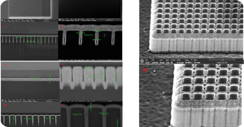
SEM process detail
Packaged semiconductor module
SEM process characterization

聯絡我們

從 AI 輔助器件設計到晶圓級製造,涵蓋壓電 MEMS、光子、III–V、寬能隙與異質材料系統。

25FAB AI 輔助工程設計

Tell 25FAB what you need

Submit a technically actionable design brief. Nothing is stored on this website: the final button prepares an email in your own email application.

Same-day paid design package

A design package can be delivered on the day payment is confirmed, once the technical brief is complete and actionable. Fabrication, qualification and custom process development follow separate schedules.

付款 → 設計
Select a family to load its professional engineering prompts.Explore the 25FAB AI Design workspace ↗
01Design brief
Required field.
The engineering examples below change with the selected design family.
02Requested deliverables
03Company / Institution
Required field.