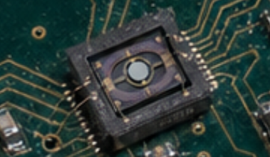
Piezoelectric beam steering
Low-voltage MEMS micromirror and array architectures for fast optical addressing and compact beam-control engines.
Wafer-level building blocks for neutral-atom control, quantum photonics and precision optical systems — combining piezoelectric beam steering, metasurfaces and integrated photonics.
25FAB develops custom wafer-level architectures for optical addressing, beam steering and integrated photonic control. Engineering routes can combine piezoelectric MEMS, metasurfaces, Si₃N₄/SOI photonics, III–V integration and packaged optical interfaces.
Low-voltage MEMS micromirror and array architectures for fast optical addressing and compact beam-control engines.
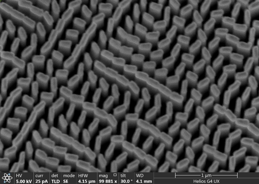
Custom wavelength, aperture, NA and wavefront engineering for beam shaping, focusing and optical addressing.
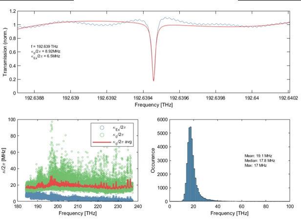
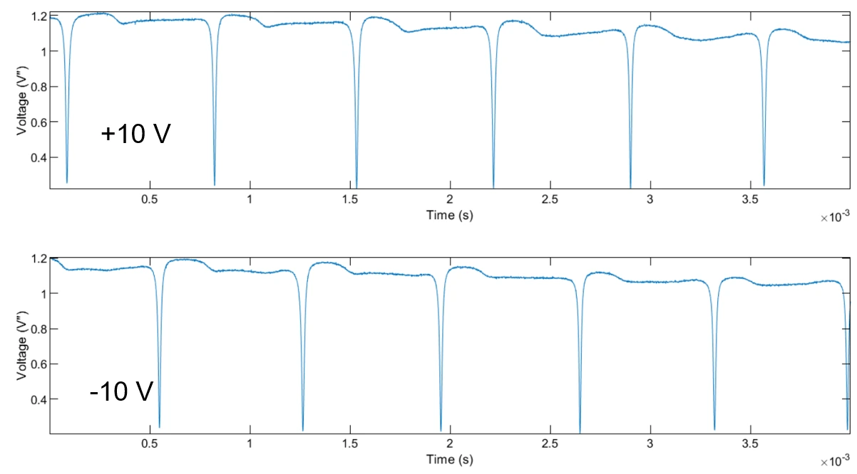
High-Q photonic devices with integrated piezoelectric actuation; measured DC tuning of 20 MHz/V on the demonstrated PIC platform.
High-Q telecom-band photonic resonances with repeatable optical response under ±10 V actuation on the demonstrated platform.
Start from the function you need. 25FAB co-designs the optical, mechanical and material stack, then carries the program through engineering wafer, measurement, packaging and scale-up.
Combine beam steering, wavefront engineering, photonic routing and packaged optical interfaces around the system function.