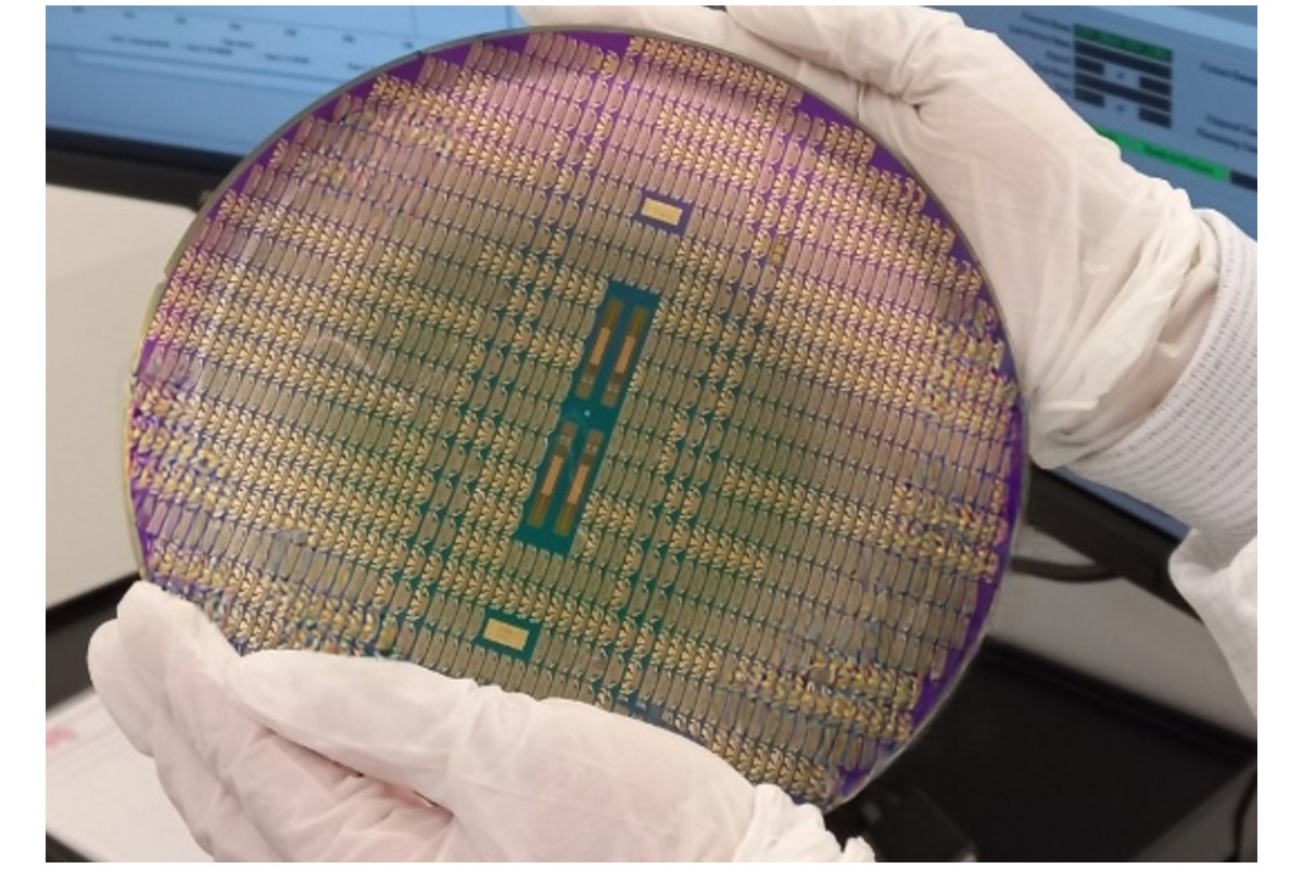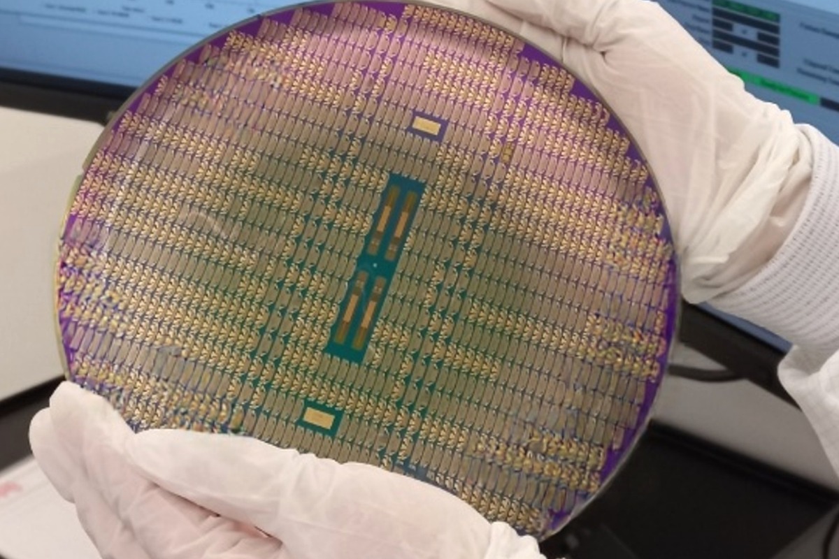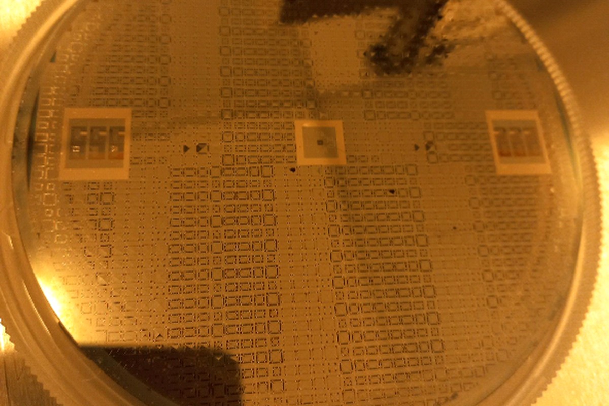
Piezoelectric MEMS Micromirrors
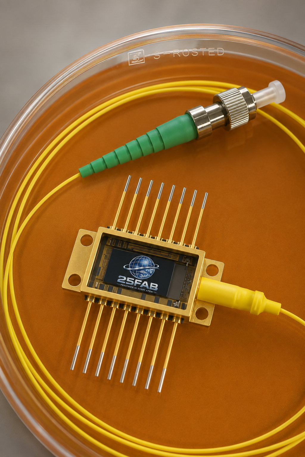
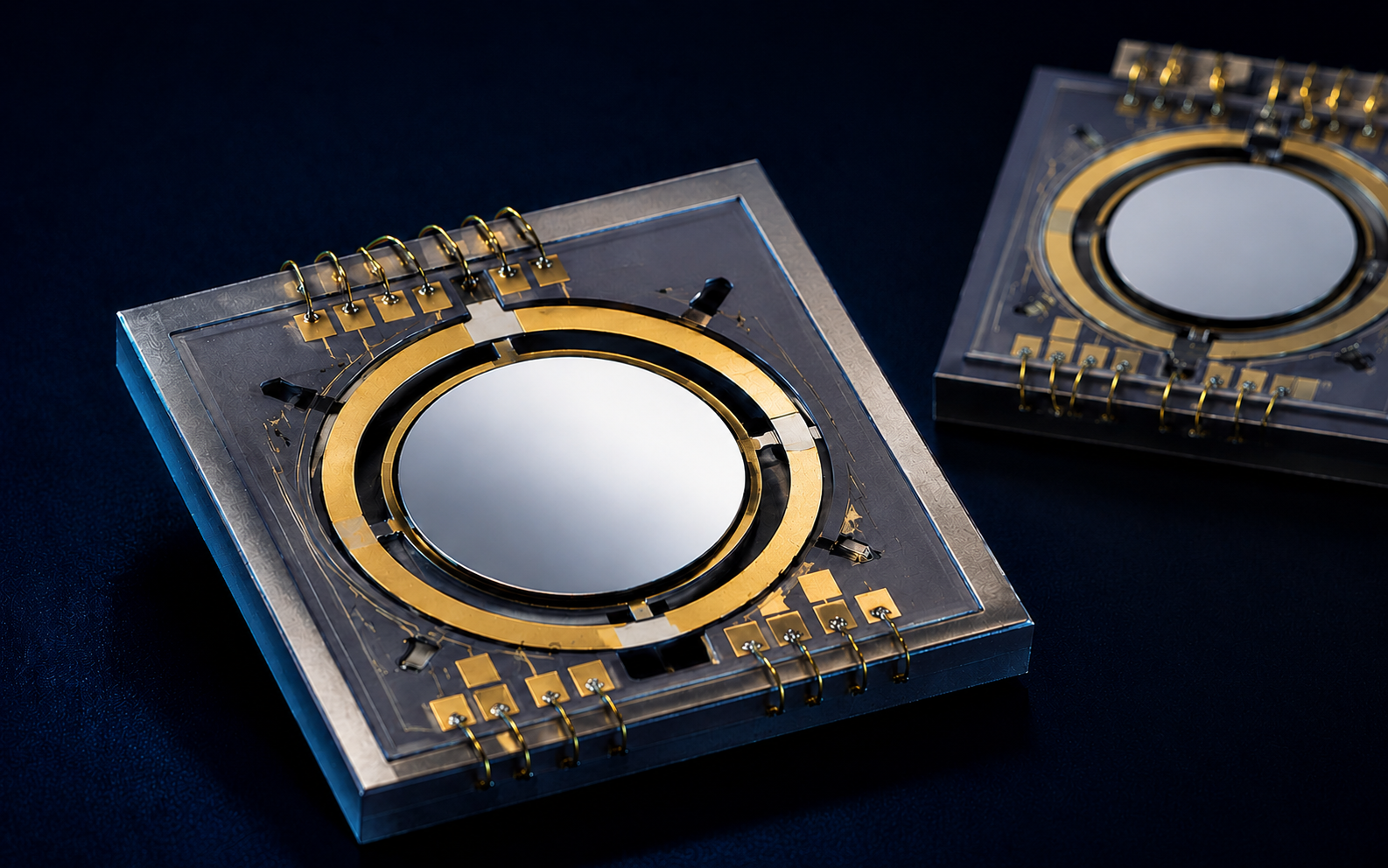
Fast, precise beam steering and optical scanning with low-voltage piezoelectric actuation.
From functional requirements to manufacturable architectures across piezoelectric, photonic, III–V and wide-bandgap systems — including monolithic multi-material integration and wafer-level scale-up.
Submit functional targets for MEMS, photonics, metasurfaces, compound semiconductors or custom devices. Our platform translates them into manufacturable architectures and multi-material integration routes.
Two commercially focused platforms that make 25FAB easy to understand at first glance.

Fast, precise beam steering and optical scanning with low-voltage piezoelectric actuation.

Five clear commercial PMUT families spanning 1–60 MHz for OEM engineering, pilot and volume programs.
Specialist manufacturing and development routes for MEMS, photonics and compound-semiconductor devices.
Configurable PMUT chips and arrays from 1–60 MHz, including OEM frequency families for engineering, pilot and volume programs.
View Platform →
Clear sound, wide bandwidth and compact piezoelectric acoustic devices.
View Platform →
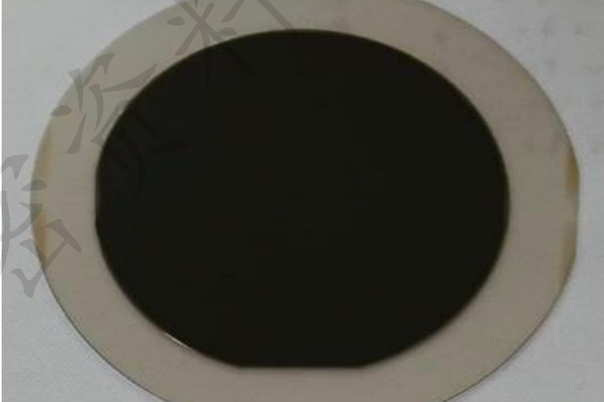
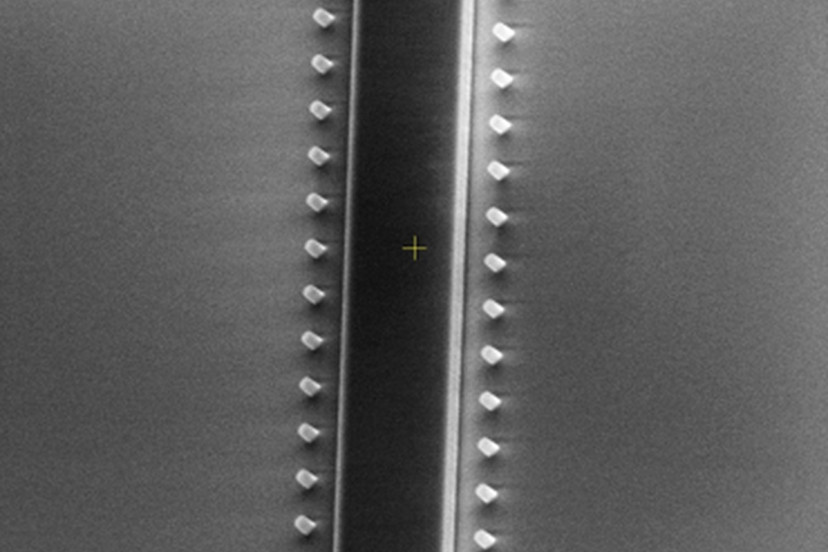
Fast, precise beam steering and optical scanning with low-voltage piezoelectric actuation.
View Platform →
Rugged semiconductor and MEMS platforms for high-power, harsh-environment and advanced sensing applications.
View Platform →
High-speed photonic and optoelectronic platforms for communication, sensing and integrated light sources.
View Platform →
Advanced III–V materials for infrared detection, sensing and integrated optoelectronics.
View Platform →
Integrated photonic circuits and wafer-level manufacturing for scalable optical systems.
View Platform →
Integrated photonics combined with piezoelectric and BTO-based functional materials for tunable optical devices, high-speed modulation and heterogeneous integration.
View Platform →
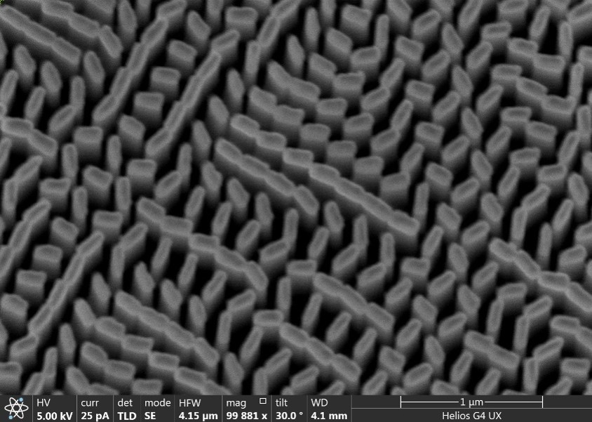
Custom flat-optics, metalens and metasurface devices for beam shaping, focusing, sensing and 3D imaging.
View Platform →
GaN-based and advanced custom semiconductor platforms for metasurfaces, photonics, sensing and project-specific integration.
View Platform →Clear project stages help OEM and deep-tech teams understand how to start and how a program can scale.
Target function, frequency, aperture, geometry, interfaces and delivery format.
Device architecture and process route are aligned with the target application.
Engineering samples or wafers provide the first physical validation point.
Pilot and dedicated wafer routes support the transition toward repeatable supply.
From functional requirements to manufacturable architectures across piezoelectric, photonic, III–V and wide-bandgap systems — including monolithic multi-material integration and wafer-level scale-up.