Engineering development · Dedicated wafer runs · Hybrid integration

InP-Plattformen

Custom indium-phosphide fabrication and integration for photonic integrated circuits, lasers, modulators, detectors and heterogeneous systems.

Hochgeschwindigkeits-Photonik und Optoelektronik für Kommunikation und Sensorik.

Active photonic devices
High-speed optoelectronics
Custom wafer-level processing
Hybrid integration routes
InP-Plattformen

Unser Lieferumfang

  • InP photonic and optoelectronic chips
  • Custom process modules
  • Active and passive device integration
  • Diced chips and wafer-level delivery
  • Test structures and process monitors
  • Dedicated development and pilot runs

Konfigurierbare Parameter

  • Epitaxial stack
  • Device architecture
  • Waveguide and active-region geometry
  • Metallisation and contacts
  • Facet and chip requirements
  • Wafer and production volume

Anwendungsbereiche

  • Optical communications
  • Integrated lasers
  • Quantum photonics
  • LiDAR and sensing
  • Microwave photonics
  • Heterogeneous PIC systems

Fertigungsweg

1

Engineering-Samples

2

Pilotproduktion

3

Serienproduktion

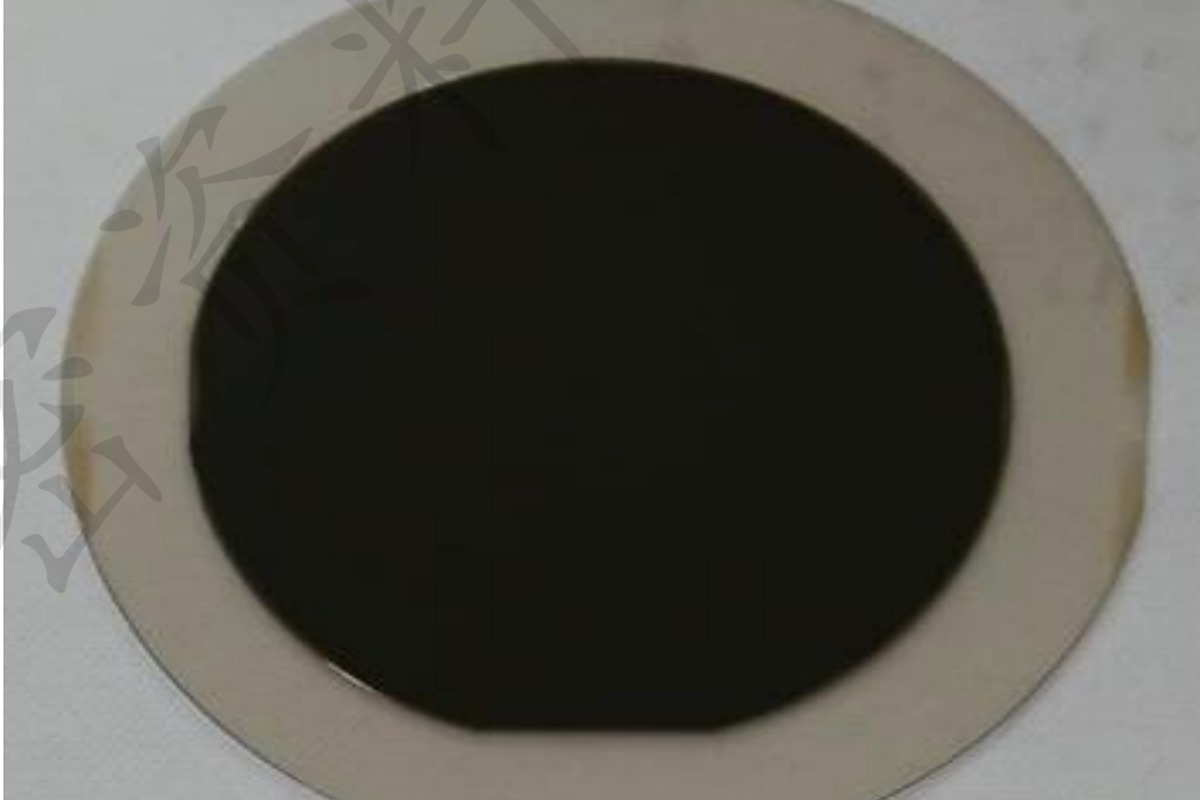
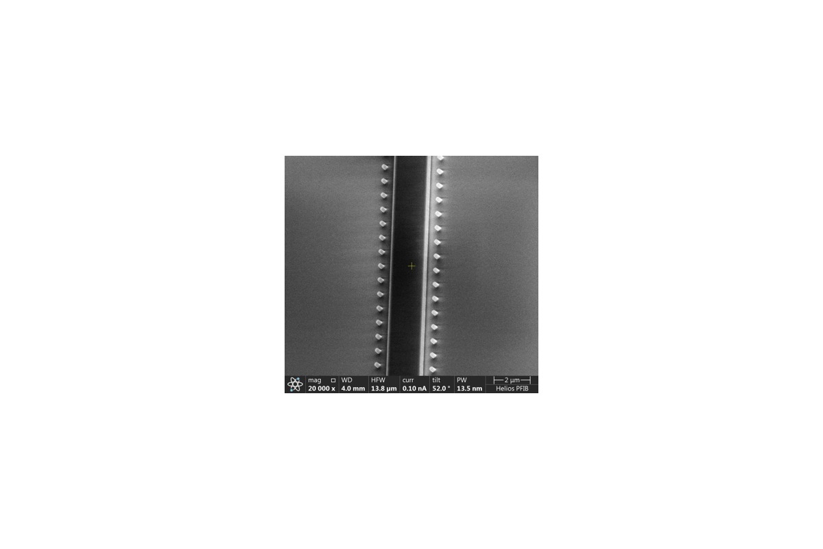
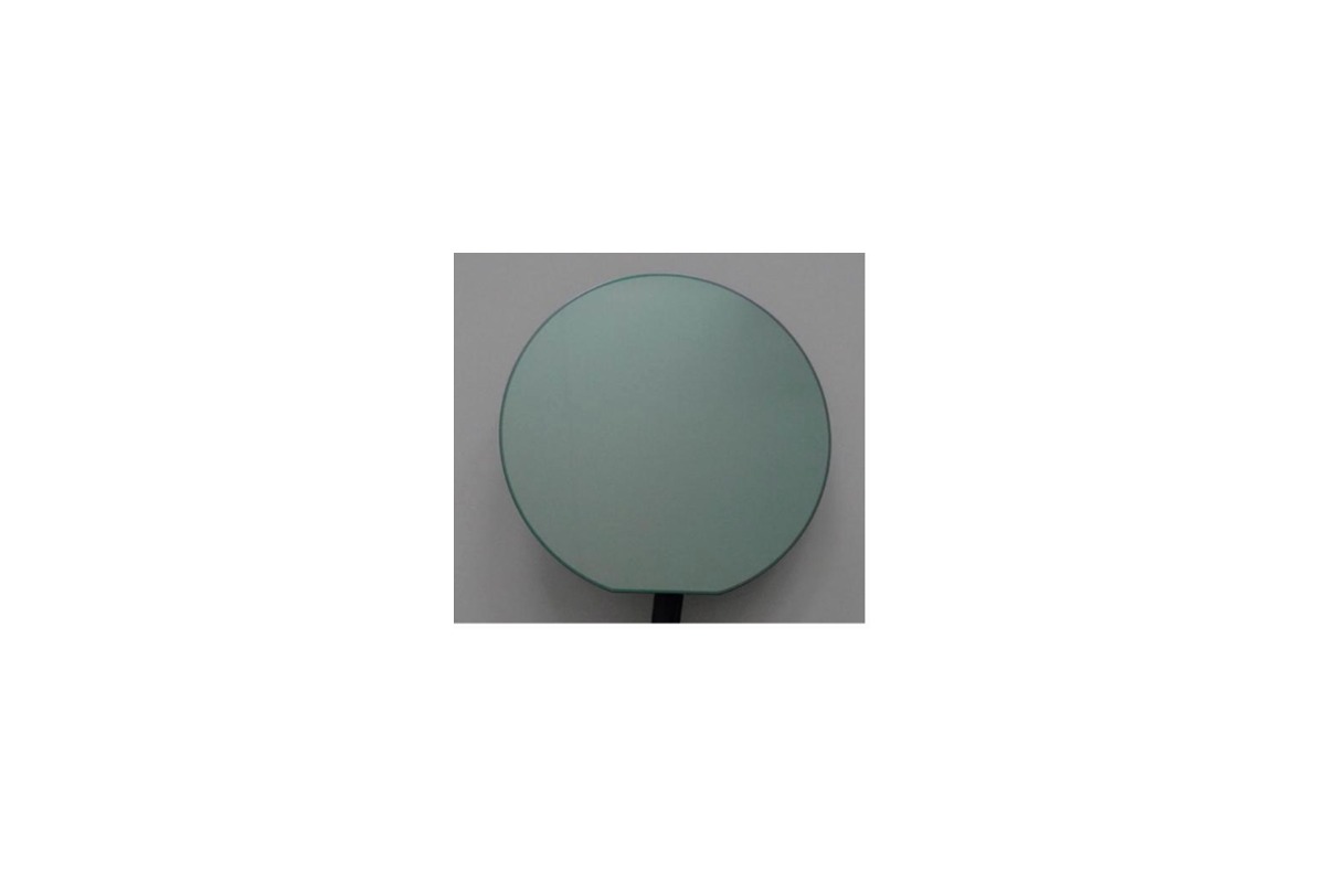
Reale Fertigung & Charakterisierung

Ausgewählte 25FAB- und projektbezogene Fertigungsbilder mit stärkerer kommerzieller Präsentation.
Kontakt

InP-Plattformen