PMUT · 126% MEASURED BANDWIDTH
PMUT OEM Module
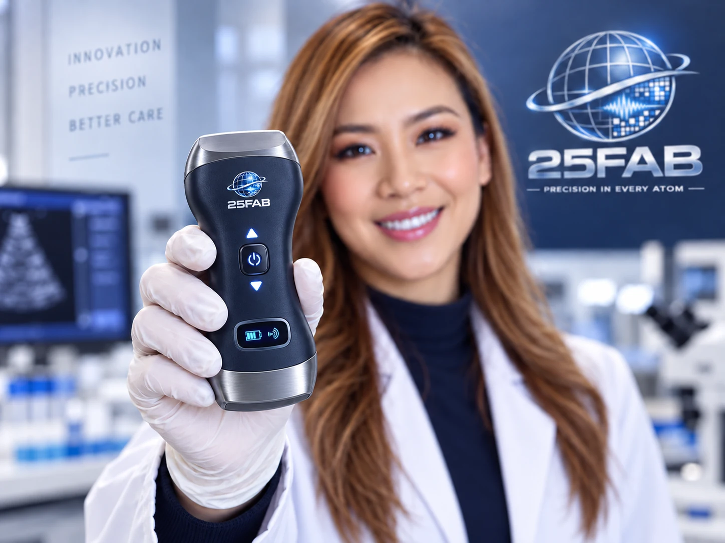
Broadband piezoelectric ultrasound from custom array design to packaged OEM integration. 126% measured bandwidth on the demonstrated platform.
Explore module →25FAB co-optimizes device physics, geometry, material stacks and fabrication constraints, integrates multiple functional materials on a common wafer-level platform, and carries programs from AI architecture to measured engineering wafers, pilot lots and recurring volume production.
Broadband piezoelectric ultrasound from custom array design to packaged OEM integration. 126% measured bandwidth on the demonstrated platform.
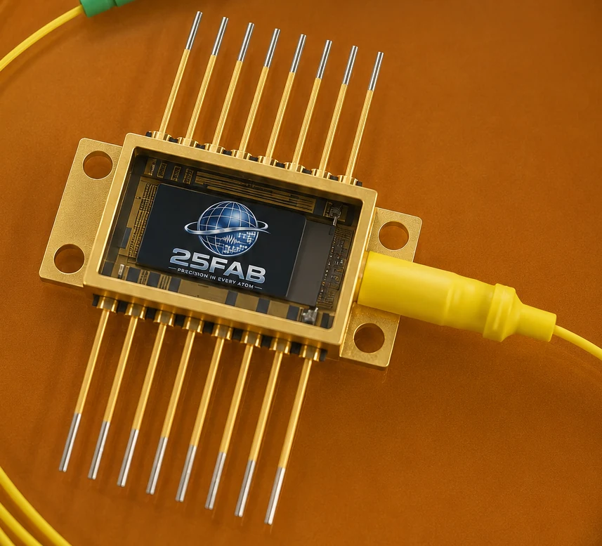
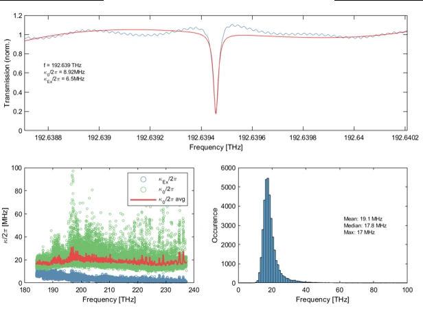
Integrated photonics with piezoelectric actuation, measured 20 MHz/V DC tuning near 1550 nm, and a route from die to packaged module.
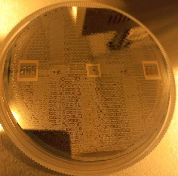
Wafer-level piezoelectric MEMS speaker with 69 dB measured acoustic output, available for custom, pilot and volume manufacturing programs.
Start with measured products. 25FAB puts PMUT, piezo-tunable PICs and the 69 dB piezo MEMS speaker first, with a dedicated module route for quantum systems.
Broadband piezoelectric ultrasound from custom array design to packaged OEM integration. 126% measured bandwidth on the demonstrated platform.
Explore module →Integrated photonics with piezoelectric actuation, measured 20 MHz/V DC tuning near 1550 nm, and a route from die to packaged module.
Explore module →Wafer-level piezoelectric MEMS speaker with 69 dB measured acoustic output, available for custom, pilot and volume manufacturing programs.
Explore module →
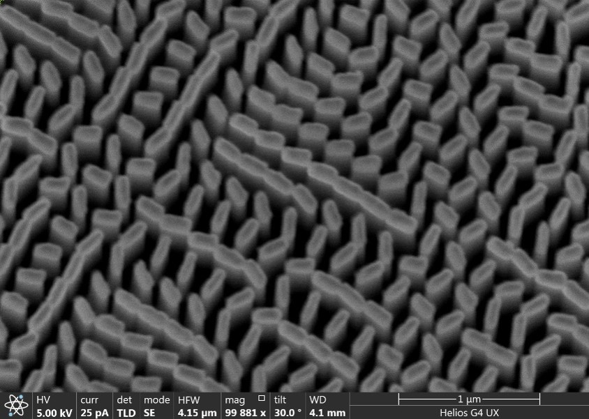
A modular wafer-level route for neutral-atom optical control, quantum photonics and precision beam systems: piezo MEMS, metasurfaces and tunable PICs.
Explore quantum systems →Not simulation alone. 25FAB closes the loop from AI design to wafer fabrication, measured device results and scalable supply.
Broadband piezoelectric ultrasound platform · custom, pilot and volume programs accepted.
Wafer-level piezoelectric MEMS speaker · custom, pilot and volume manufacturing accepted.
Piezo-tunable PIC near 1550 nm · repeatable response under +10 V / −10 V actuation.
Selected programs: design freeze → wafer fabrication → measurement → design feedback.
Broadband piezoelectric ultrasound platform · custom, pilot and volume programs accepted.
PILOT + VOLUME PROGRAMSWafer-level piezoelectric MEMS speaker · custom, pilot and volume manufacturing accepted.
PILOT + VOLUME PROGRAMS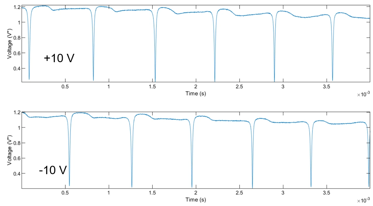
Piezo-tunable PIC near 1550 nm · repeatable response under +10 V / −10 V actuation.
PILOT + VOLUME PROGRAMSSubmit functional targets for MEMS, photonics, metasurfaces, compound semiconductors or custom devices. Our platform translates them into manufacturable architectures and multi-material integration routes.
25FAB supports project-specific design and wafer processing across piezoelectric, photonic, III–V, wide-bandgap and heterogeneous material systems.
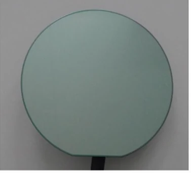
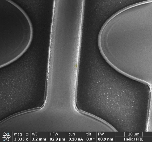
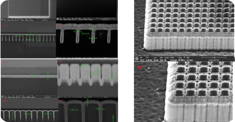
Specialist manufacturing and development routes for MEMS, photonics and compound-semiconductor devices.
Industrial PMUT chips and arrays aligned to 1–5, 2–6, 3–10, 4–13, 5–15, 8–20 and 1–15 MHz OEM architectures.
View Platform →
Clear sound, wide bandwidth and compact piezoelectric acoustic devices.
View Platform →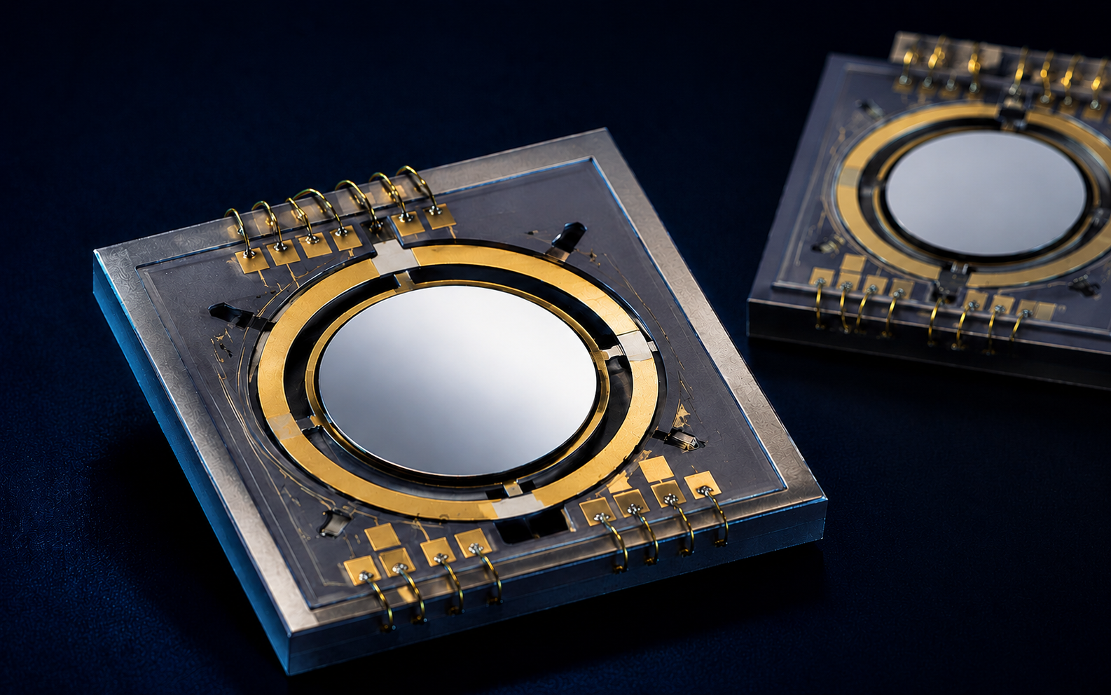
Fast, precise beam steering and optical scanning with low-voltage piezoelectric actuation.
View Platform →
Rugged semiconductor and MEMS platforms for high-power, harsh-environment and advanced sensing applications.
View Platform →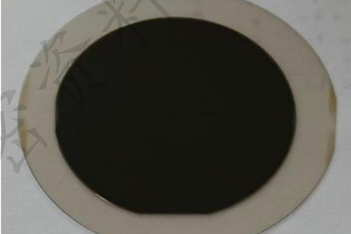
High-speed photonic and optoelectronic platforms for communication, sensing and integrated light sources.
View Platform →
Advanced III–V materials for infrared detection, sensing and integrated optoelectronics.
View Platform →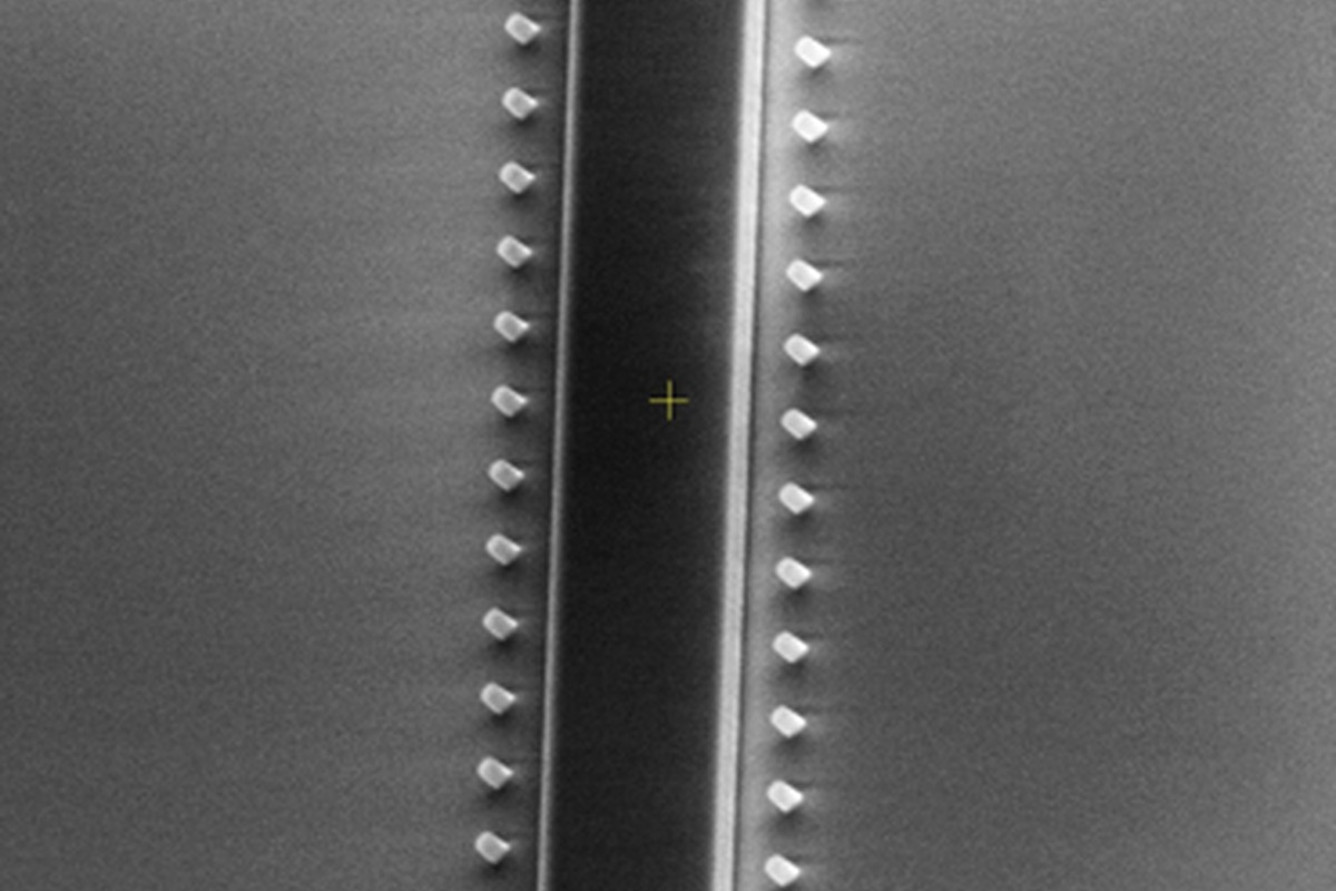
Integrated photonic circuits and wafer-level manufacturing for scalable optical systems.
View Platform →
PIC integration with PZT, AlN, AlScN, BTO-on-Si and other electro-optic / piezoelectric functional films.
View Platform →
Custom flat-optics, metalens and metasurface devices for beam shaping, focusing, sensing and 3D imaging.
View Platform →
Project-specific semiconductor and heterogeneous-integration routes for GaN, GaAs, Ge-on-Si, GeSn, diamond and non-standard material stacks.
View Platform →Every supported 25FAB platform can be engaged from custom NRE and engineering wafers through pilot, qualification and recurring production, subject to process qualification and customer specifications.
AI design → multi-material integration → engineering wafer → measured validation → pilot → volume production
Clear project stages help OEM and deep-tech teams understand how to start and how a program can scale.
Target function, frequency, aperture, geometry, interfaces and delivery format.
Device architecture and process route are aligned with the target application.
Engineering samples or wafers provide the first physical validation point.
Pilot and dedicated wafer routes support the transition toward repeatable supply.
AI co-design, multi-material monolithic integration, measured device performance and a direct path from engineering wafers to pilot and volume manufacturing.